Liquid crystal display device

a display device and liquid crystal technology, applied in liquid crystal compositions, instruments, chemistry apparatus and processes, etc., can solve the problems of low reliability of oxide semiconductor thin-film transistors, strict impurity control, electrical characteristics of display devices, etc., to achieve the effect of reducing the voltage holding ratio (vhr), increasing the ion density (id), and consuming less power

Inactive Publication Date: 2016-09-22
DAINIPPON INK & CHEM INC
View PDF4 Cites 9 Cited by
  • Summary
  • Abstract
  • Description
  • Claims
  • Application Information

AI Technical Summary

Benefits of technology

[0016]The liquid crystal display device according to the present invention, which includes oxide semiconductor TFTs and a particular liquid crystal composition, does not exhibit a significant decrease in voltage holding ratio (VHR) or increase in ion density (ID) of the liquid crystal layer and thus does not suffer from display defects such as white spots, uneven alignment, and image-sticking and also consumes less power.

Problems solved by technology

Unfortunately, oxide semiconductor thin-film transistors have low reliability due to variations in electrical characteristics.
The variations in electrical characteristics are attributable to lattice defects, such as oxygen defects, which occur when oxygen desorbs from an oxide semiconductor layer.
A liquid crystal composition used for a liquid crystal layer of a liquid crystal display device is subjected to strict impurity control since impurities present in the composition greatly affect the electrical characteristics of the display device.
Although research has been conducted on various solutions to the problem of lattice defects such as oxygen defects, as discussed in PTL 2, they have been unsuccessful in sufficiently reducing the desorption of oxygen from an oxide semiconductor layer.
A typical liquid crystal display device includes only a thin insulating layer, or a thin insulating layer and a thin alignment layer, between oxide semiconductor layers of thin-film transistors and a liquid crystal layer to separate the liquid crystal composition from the oxide semiconductor layer; therefore, the diffusion of oxygen desorbed from the oxide semiconductor layer and the resulting alteration of the insulating layer result in insufficient separation of the liquid crystal layer from the oxide semiconductor layer.
The diffusion of impurities such as oxygen desorbed from the oxide semiconductor layer into the liquid crystal layer may decrease the voltage holding ratio (VHR) and increase the ion density (ID) of the liquid crystal layer and may thus cause display defects such as white spots, uneven alignment, and image-sticking.
However, as disclosed in PTL 2, the previous inventions are intended to reduce the desorption of oxygen from oxide semiconductors; no research has been conducted on the direct relationship between oxide semiconductor thin-film transistors and liquid crystal compositions.

Method used


Image

  • Liquid crystal display device
  • Liquid crystal display device
  • Liquid crystal display device

Examples


first embodiment

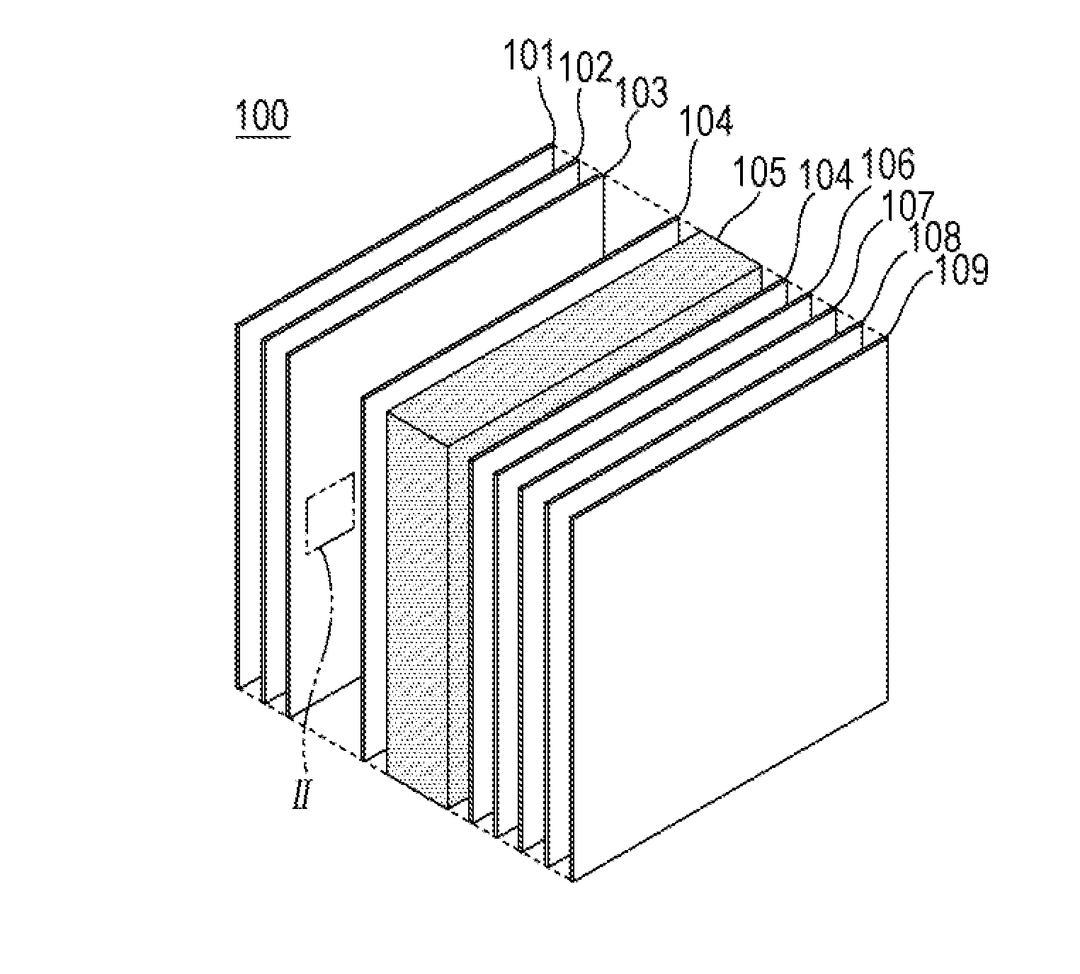
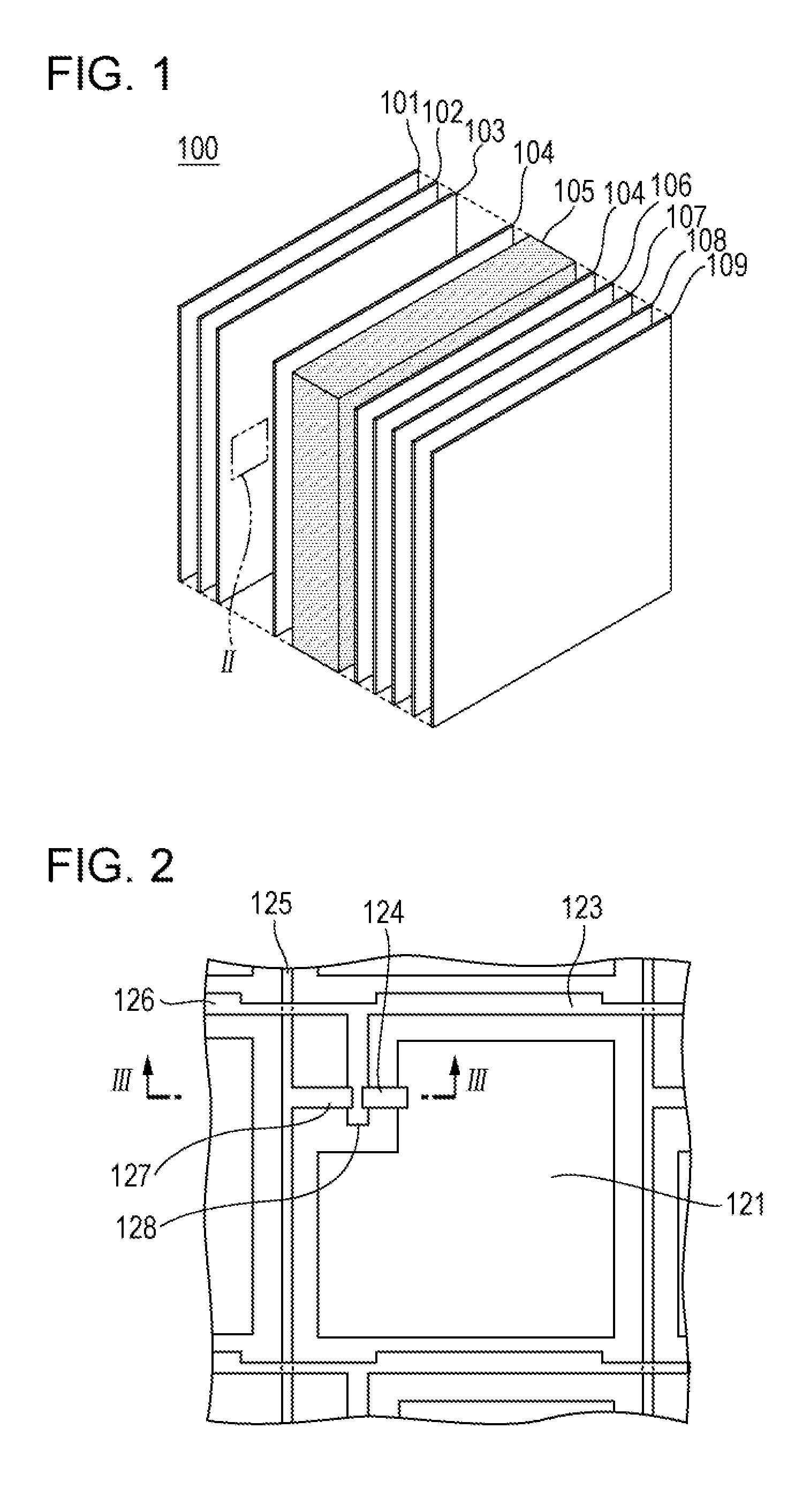
[0028]A liquid crystal display device according to a first preferred embodiment of the present invention includes oxide semiconductor thin-film transistors and a particular liquid crystal composition and generates a substantially perpendicular electric field between first and second substrates. The liquid crystal display device according to the first preferred embodiment is a liquid crystal display device having electrodes on both first and second substrates, for example, a vertically aligned (VA) transmissive liquid crystal display device.

[0029]The liquid crystal display device according to the first preferred embodiment of the present invention preferably includes first and second opposing substrates, a liquid crystal layer containing a liquid crystal composition between the first and second substrates, a plurality of gate bus lines and data bus lines arranged in a matrix on the first substrate, thin-film transistors disposed at intersections of the gate bus lines and the data bus...

second embodiment

[0204]A liquid crystal display device according to a second embodiment of the present invention includes oxide semiconductor thin-film transistors and a particular liquid crystal composition and generates an electric field containing a component parallel to the substrate surface. The liquid crystal display device according to the second preferred embodiment is an in-plane switching (IPS) liquid crystal display device or a fringe-field switching (FFS) liquid crystal display device, which is a type of IPS liquid crystal display device.

[0205]An IPS liquid crystal display device according to the second preferred embodiment of the present invention preferably includes first and second opposing substrates, a liquid crystal layer containing a liquid crystal composition between the first and second substrates, a plurality of gate lines and data lines arranged in a matrix on the first substrate, thin-film transistors disposed at intersections of the gate lines and the data lines, and pixel e...

third embodiment

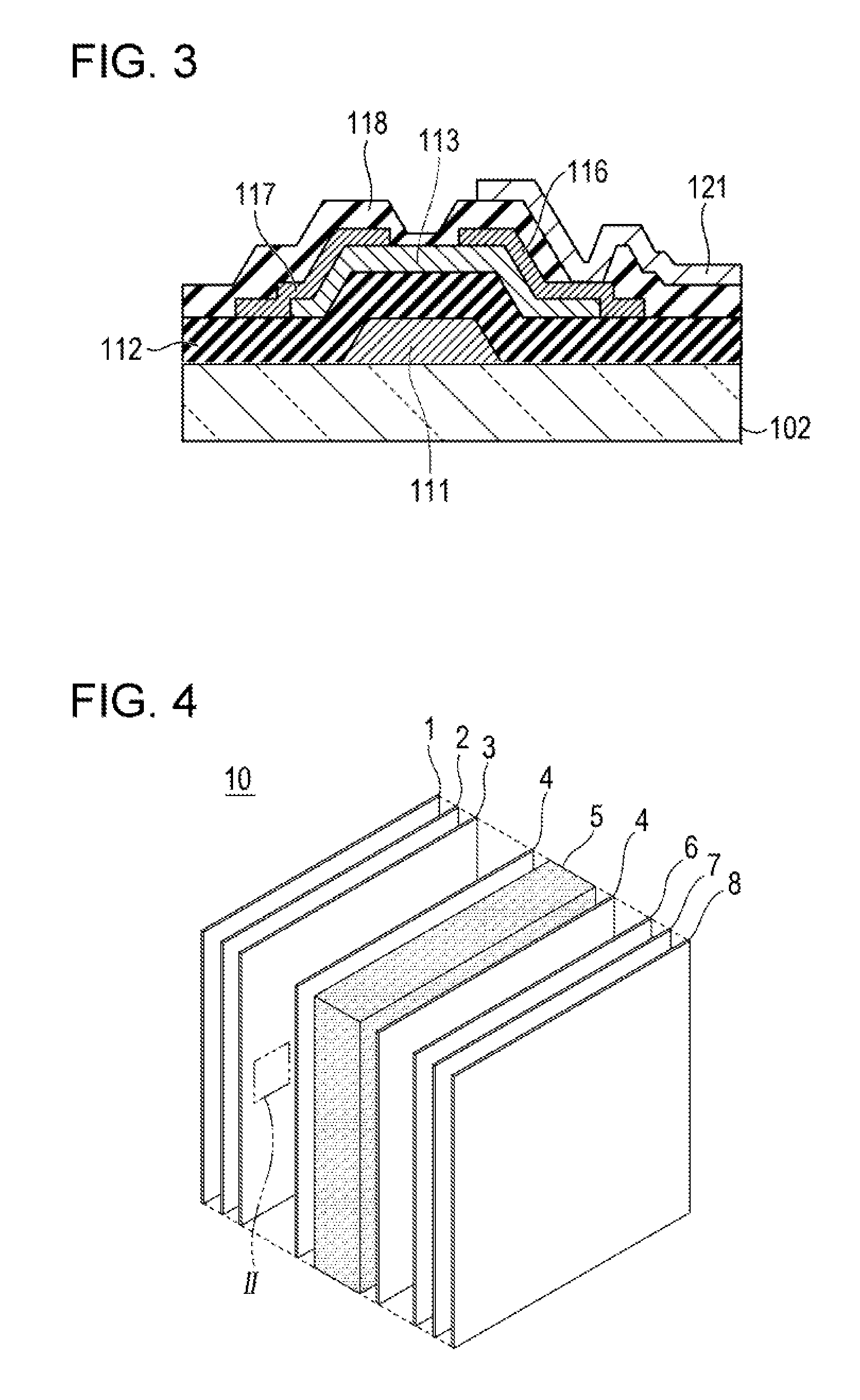
[0226]A liquid crystal display device according to a third embodiment of the present invention includes oxide semiconductor thin-film transistors and a particular liquid crystal composition. The liquid crystal display device preferably includes color filters 6 formed on the same substrate as the electrode layer 3 including the thin-film transistors, i.e., on the first substrate. This structure is commonly known as color-filter-on-array (COA). Specific structures will now be described with reference to FIGS. 10 and 11. FIG. 10 is another example of a sectional view of a liquid crystal display device. A first substrate 2 having an alignment layer 4, thin-film transistors (11, 13, 15, 16, and 17), color filters 6, and pixel electrodes 21 formed thereon and a second substrate 7 having an alignment layer 4 formed thereon are separated from each other such that the alignment layers 4 face each other. This space is filled with a liquid crystal layer 5 containing a liquid crystal compositio...


PUM

PropertyMeasurementUnit
temperatureaaaaaaaaaa
resistivityaaaaaaaaaa

Abstract

Provided is a liquid crystal display device including first and second opposing substrates, a liquid crystal layer containing a liquid crystal composition between the first and second substrates, thin-film transistors disposed on the first substrate, and pixel electrodes that are driven by the transistors and that are made of a transparent conductive material. Each thin-film transistor includes a gate electrode, an oxide semiconductor layer disposed over the gate electrode with an insulating layer therebetween, and source and drain electrodes electrically connected to the oxide semiconductor layer. The liquid crystal composition contains at least one compound selected from the group consisting of compounds represented by general formulas (LC3) to (LC5) and at least one compound selected from the group consisting of compounds represented by general formulas (II-a) to (II-f).

Description

TECHNICAL FIELD[0001]The present invention relates to liquid crystal display devices.BACKGROUND ART[0002]Liquid crystal display devices are used in various products, including clocks, calculators, household electrical appliances, measuring instruments, automotive instrument panels, word processors, electronic organizers, printers, computers, and televisions. Typical types of liquid crystal display devices include twisted nematic (TN), super-twisted nematic (STN), dynamic scattering (DS), guest-host (GH), in-plane switching (IPS), fringe-field switching (FFS), optically compensated birefringence (OCB), electrically controlled birefringence (ECB), vertically aligned (VA), color super-homeotropic (CSH), and ferroelectric liquid crystal (FLC) display devices. Although conventional liquid crystal display devices are statically driven, multiplexed liquid crystal display devices have been commonly used. Among the mainstream schemes are passive-matrix driving and, more recently, active-matr...

Claims


Application Information

Patent Timeline
Patent Type & Authority Applications(United States)
IPC IPC(8): C09K19/30G02F1/1337G02F1/1333G02F1/1343G02F1/1362G02F1/1368
CPCC09K19/3003G02F1/136286G02F1/1368G02F1/133365G02F1/13439G02F1/1337G02F2001/133738C09K2019/3004C09K2019/3009C09K2019/301C09K2019/3016G02F2202/10G02F2001/133746G02F1/134309C09K19/0403C09K19/322C09K2019/0448C09K2019/325G02F1/133738G02F1/133746
Inventor OGAWAIWASHITA, YOSHINORI
Owner DAINIPPON INK & CHEM INC
Why Eureka
Try Eureka