Interposers for integrated circuits with multiple-time programming and methods for manufacturing the same

a technology of integrated circuits and programming, applied in the direction of magnetic field-controlled resistors, electrical devices, semiconductor devices, etc., can solve the problems of programming creating permanent changes to silicon, lack of peripheral chips from main controller chips,

a technology of integrated circuits and programming, applied in the direction of magnetic field-controlled resistors, electrical devices, semiconductor devices, etc., can solve the problems of programming creating permanent changes to silicon, lack of peripheral chips from main controller chips,

US20160343773A1Active Publication Date: 2016-11-24GLOBALFOUNDRIES SINGAPORE PTE LTD

Image

  • Interposers for integrated circuits with multiple-time programming and methods for manufacturing the same
  • Interposers for integrated circuits with multiple-time programming and methods for manufacturing the same
  • Interposers for integrated circuits with multiple-time programming and methods for manufacturing the same

Examples


Embodiment Construction

[0014]The following detailed description is merely exemplary in nature and is not intended to limit the various embodiments and uses thereof. Furthermore, there is no intention to be bound by any theory presented in the preceding background or the following detailed description.

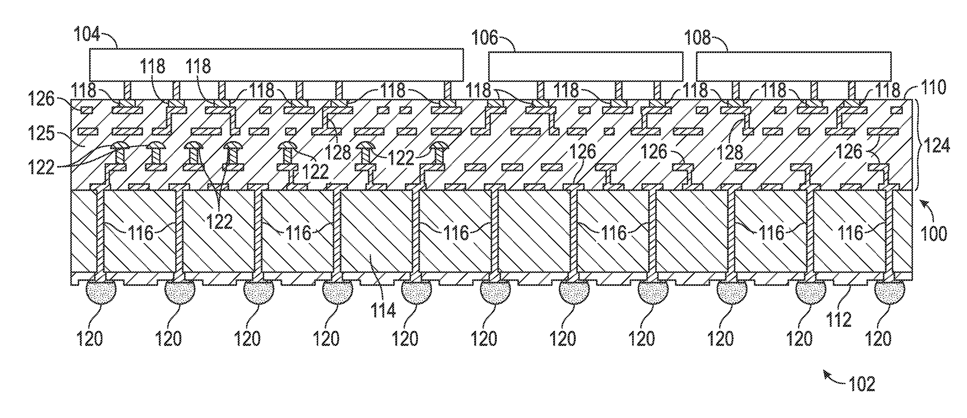
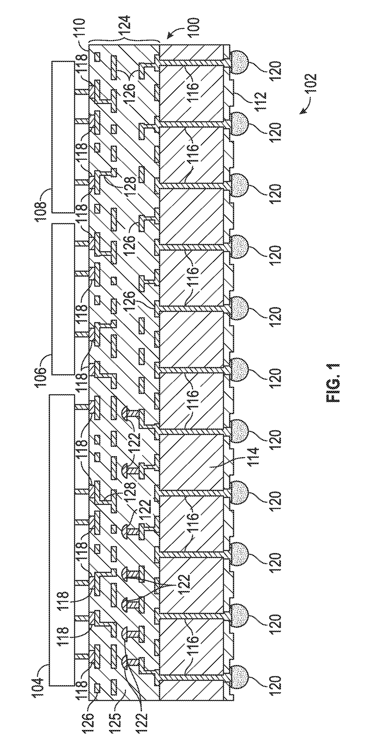
[0015]Referring to the figures, wherein like numerals indicate like parts throughout the several views, an interposer 100 for an integrated circuit 102 and method 500 of manufacturing the interposer 100 is shown and described herein.

[0016]Referring to FIG. 1, the integrated circuit 102 within which the interposer 100 may be utilized may be a three-dimensional (“3D”) integrated circuit, a 2.5D integrated circuit, or other appropriate “stacked” integrated circuits as appreciated by those skilled in the art. The exemplary integrated circuit 102 shown in FIG. 1 includes a first chip 104, a second chip 106, and a third chip 108 electrically connected to the interposer 100. However, it should be appreciated that an...


PUM


Abstract

An interposer for an integrated circuit includes a first side and a second side. The interposer includes a substrate and a via disposed in the substrate. A first electrical contact is disposed on the first side. A second electrical contact is disposed on the second side and electrically connected to the via. The interposer also includes a multiple-time programmable (“MTP”) element electrically connected to the first electrical contact and / or the via.

Description

TECHNICAL FIELD[0001]The technical field relates generally to interposers for integrated circuits and methods for manufacturing such interposers, and more particularly to 3D integrated circuits with interposers with integrated multiple-time programming capabilities and methods for manufacturing such integrated circuits.BACKGROUND[0002]In many 3D integrated circuits, transistor-based memory cells utilize fuses, thus making the memory cells “one-time programmable”. One issue with the use of such fused memory cells is that the programming creates permanent changes to the silicon, which can be easily detected and reversed engineered with physical inspection.[0003]Another issue with 3D integrated circuits is the lack of control of peripheral chips from a main controller chip. Often times, these peripheral chips are always powered up and running, even when not necessary.[0004]As such, it is desirable to provide an interposer for an integrated circuit that allows for multiple-time programm...

Claims


Application Information

Patent Timeline
24 Nov 2016
Publication
US20160343773A1
IPC
H01L27/24; H01L43/12; H01L43/08; H01L27/22; H01L45/00
CPC
H01L27/2436; H01L27/228; H01L45/06; H01L43/12; H01L43/08; H01L45/16; H01L45/144; H01L2224/16225
Inventors
TAN, JUAN BOON; JIANG, YI