Semiconductor device including metal-2 dimensional material-semiconductor contact

a two-dimensional material and contact technology, applied in the field of semiconductor devices, can solve the problems of limit in reducing the schottky energy barrier regardless of a metal type, limit in the method of increasing the concentration of doping

Active Publication Date: 2016-11-24
SAMSUNG ELECTRONICS CO LTD
View PDF55 Cites 16 Cited by
  • Summary
  • Abstract
  • Description
  • Claims
  • Application Information

AI Technical Summary

Benefits of technology

[0022]A doping concentration of each of the source region a

Problems solved by technology

However, because a phenomenon occurs when a work function of a metal is pinned on a surface of a semiconductor, there is a limit in reducing the Schottky energy barrier regardless of a type of the metal.
However, although a doping concentration needs to be further increase

Method used


Image

  • Semiconductor device including metal-2 dimensional material-semiconductor contact
  • Semiconductor device including metal-2 dimensional material-semiconductor contact
  • Semiconductor device including metal-2 dimensional material-semiconductor contact

Examples


Embodiment Construction

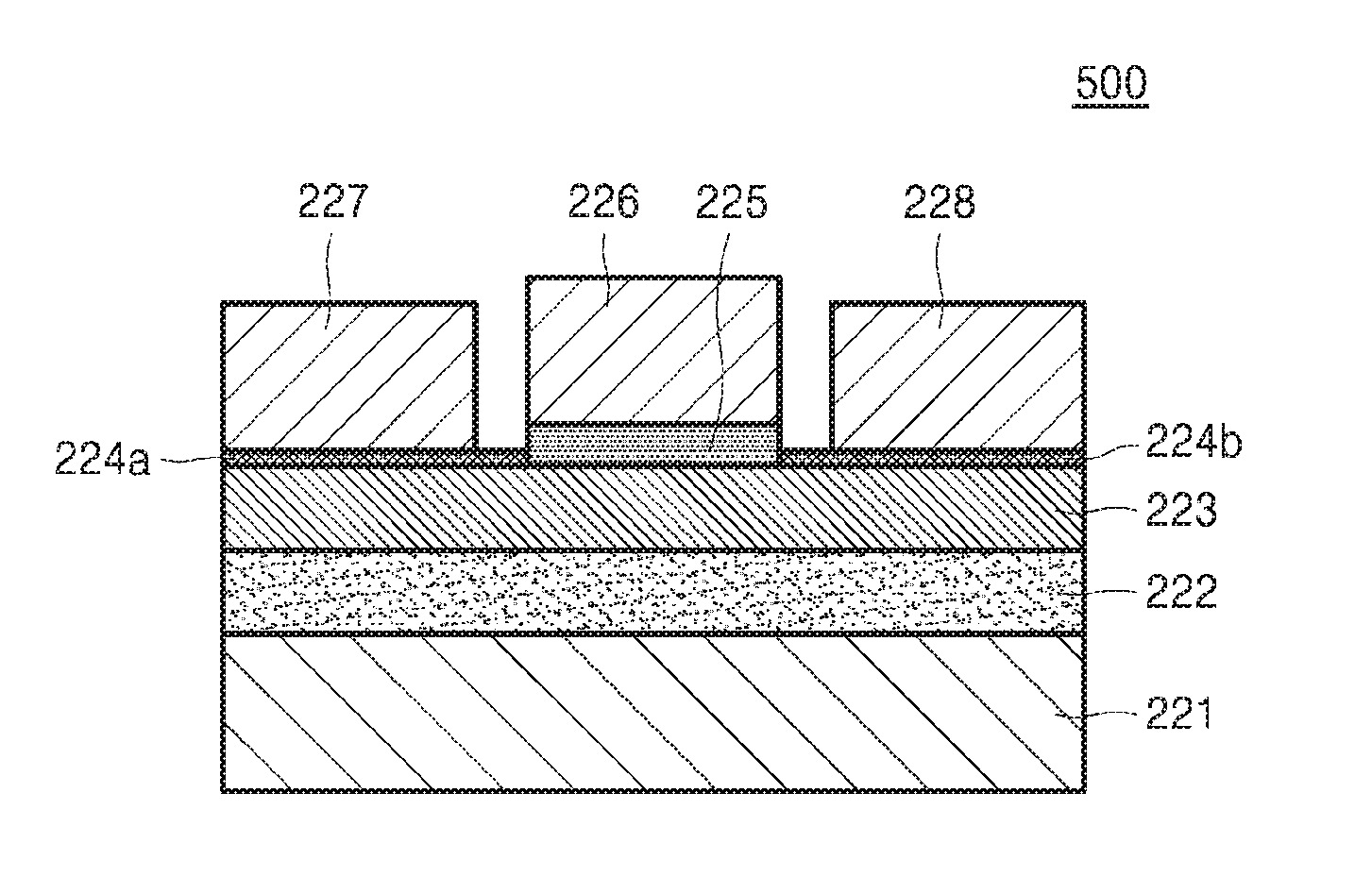
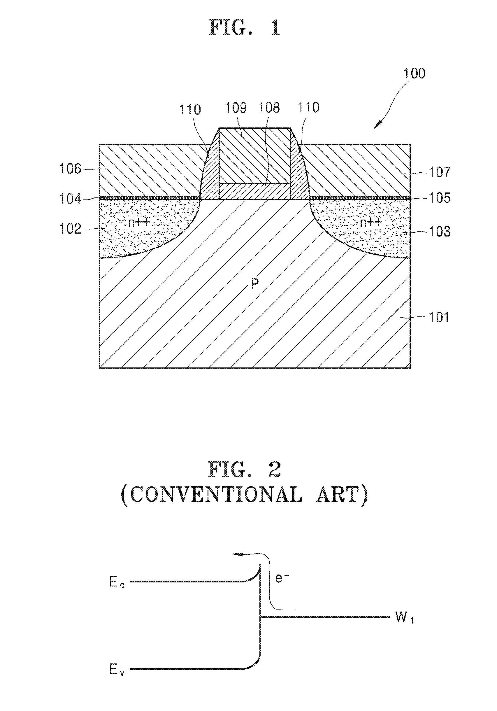
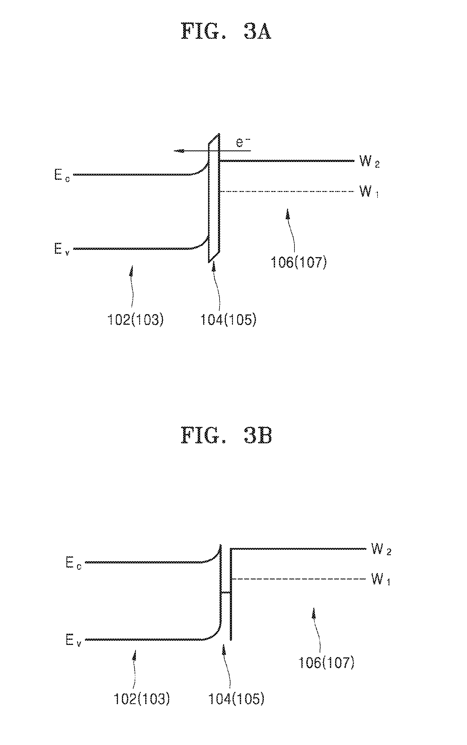
[0040]Reference will now be made in detail to a semiconductor device including contact of metal-two dimensional material-semiconductor, examples of which are illustrated in the accompanying drawings, wherein like reference numerals refer to like elements throughout. Also, the size of each layer illustrated in the drawings may be exaggerated for convenience of explanation and clarity. In this regard, the present embodiments may have different forms and should not be construed as being limited to the descriptions set forth herein. Accordingly, the embodiments are merely described below, by referring to the figures, to explain aspects of the present description. In a layer structure, when a constituent element is disposed “above” or “on” to another constituent element, the constituent element may be only directly on the other constituent element or above the other constituent elements in a non-contact manner.

[0041]It will be understood that when an element is referred to as being “on,”...


PUM


Abstract

A semiconductor device includes a semiconductor layer, a metal layer electrically contacting the semiconductor layer, and a two-dimensional material layer between the semiconductor layer and the metal layer and having a two-dimensional crystal structure.

Description

CROSS-REFERENCE TO RELATED APPLICATION[0001]This application claims the benefit of Korean Patent Application No. 10-2015-0070567, filed on May 20, 2015, and Korean Patent Application No. 10-2015-0110233, filed on Aug. 4, 2015, in the Korean Intellectual Property Office, the disclosures of each of which are incorporated herein in their entirety by reference.BACKGROUND[0002]1. Field[0003]Example embodiments relate to a semiconductor device, and more particularly, to a semiconductor device including a two-dimensional material layer that has a two-dimensional crystal structure and is interposed between a metal and a semiconductor to reduce a contact resistivity therebetween.[0004]2. Description of the Related Art[0005]A semiconductor device includes a metal and a semiconductor that are in contact with each other in a particular part of the semiconductor device to externally exchange electric signals. The metal has a lower resistivity than the semiconductor and can be more easily wired t...

Claims


Application Information

Patent Timeline
IPC IPC(8): H01L29/08H01L29/06H01L29/04H01L29/165H01L29/78H01L29/267
CPCH01L29/0847H01L29/78H01L29/267H01L29/0669H01L29/165H01L29/0665H01L29/04H01L29/06H01L21/28512H01L29/45H01L29/41725H01L29/1606H01L21/02527H01L21/0262H01L21/02491H01L21/02595H01L29/7782
Inventor LEE, MINHYUNKIM, HAERYONGSHIN, HYEONJINNAM, SEUNGGEOLPARK, SEONGJUN
Owner SAMSUNG ELECTRONICS CO LTD
Why Eureka
Try Eureka