
Controllable indium doping for high efficiency czts thin-film solar cells

a solar cell, high-efficiency technology, applied in the field of photovoltaic devices, can solve the problems of limited very large-scale deployment of this technology, several major limitations of cztsse solar cells, and low fill factor of cztsse, so as to increase junction potential and junction potential

Inactive Publication Date: 2016-12-08
IBM CORP
View PDF5 Cites 0 Cited by
  • Summary
  • Abstract
  • Description
  • Claims
  • Application Information

AI Technical Summary

Benefits of technology

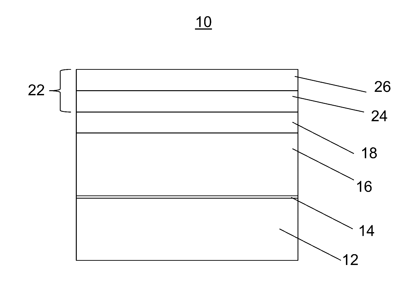
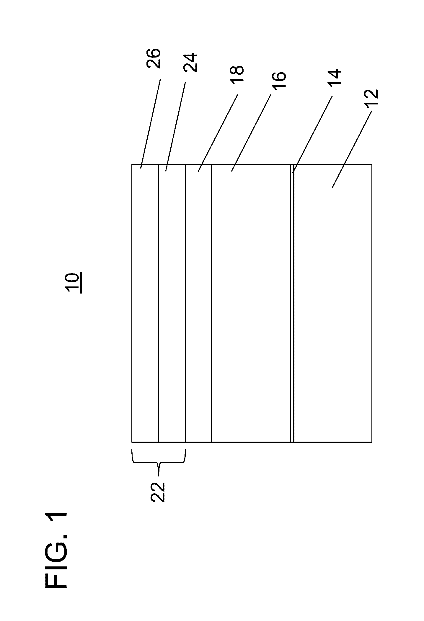
The patent describes a photovoltaic device that uses a special combination of materials to improve its performance. The device includes a layer of copper-azurium-salt (CZTSSe) on a substrate, which is followed by a layer of CdS buffer layer. The device also includes metal dopants that enhance the junction between the absorber layer and buffer layer, resulting in a more favorable potential. This leads to a higher conversion of sunlight into electrical energy. The device also includes a transparent conductive contact layer, which allows for better electrical connection. Overall, this design improves the performance of photovoltaic devices by increasing sunlight absorption and reducing the loss of electrical energy.

Problems solved by technology

Unfortunately the reliance on rare elements, such as indium, for example, limits very large scale deployment of this technology.
Several major limitations in CZTSSe solar cells exist as well.
Furthermore, CZTSSe also suffers from low fill factor (FF) which is mostly due to low Voc and higher series resistance from various layers or potential barrier formation across the device.

Method used


Image

  • Controllable indium doping for high efficiency czts thin-film solar cells
  • Controllable indium doping for high efficiency czts thin-film solar cells
  • Controllable indium doping for high efficiency czts thin-film solar cells

Examples


Embodiment Construction

[0021]In accordance with the present principles, a Cue (Zn,Sn)(S,Se)4 (CZTSSe) photovoltaic device is provided that includes benefits of earth-abundant constituent elements of the CZTSSe and may provide higher performance than conventional CZTSSe devices. The CZTSSe may be grown as a single crystal and transferred to a substrate where it can be employed as an absorber layer in a photovoltaic device, such as, e.g., a solar cell. In other embodiments, the CZTSSe (polycrystalline) may be formed on a Mo coated substrate. Single crystal CZTSSe devices may provide higher power conversion efficiency.

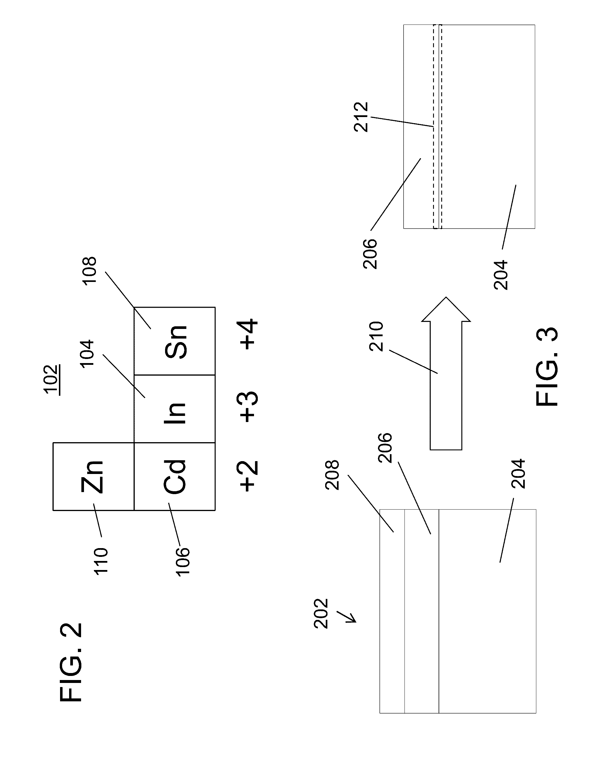
[0022]In one illustrative embodiment, a buffer layer may include CdS or other material formed on the CZTSSe layer. In accordance with the present principles, a thin indium metal layer is formed, e.g., by thermal evaporation, on the buffer layer and then diffused by an anneal process. The indium diffuses into the CdS / CZTSSe junction to enhance the operating parameters of the device.

[0023]It is t...


PUM

PropertyMeasurementUnit
thicknessaaaaaaaaaa
thicknessaaaaaaaaaa
thicknessaaaaaaaaaa

Abstract

A photovoltaic device includes a first contact layer formed on a substrate. An absorber layer includes Cu—Zn—Sn—S(Se) (CZTSSe) on the first contact layer. A buffer layer is formed in contact with the absorber layer. Metal dopants are dispersed in a junction region between the absorber layer and the buffer layer. The metal dopants have a valence between the absorber layer and the buffer layer to increase junction potential. A transparent conductive contact layer is formed over the buffer layer.

Description

RELATED APPLICATION DATA[0001]This application is a Continuation application of co-pending U.S. patent application Ser. No. 14 / 728,364 filed on Jun. 2, 2015, incorporated herein by reference in its entirety.BACKGROUND[0002]Technical Field[0003]The present invention relates to photovoltaic devices and methods for making the same, and more particularly to a solar cell with doping at a CdS / CZTS interface.[0004]Description of the Related Art[0005]Cu—In—Ga—S / Se (CIGSSe) technology provides high performance solar cells with very high power conversion efficiency (PCE) (e.g., about 20%). CIGSSe solar cells have a very large open circuit voltage (Voc) relative to bandgap with no known issues of interface recombination. Unfortunately the reliance on rare elements, such as indium, for example, limits very large scale deployment of this technology.[0006]Cu—Zn—Sn—S / Se (CZTSSe) is an emerging thin film solar cell technology consisting of all earth abundant elements. While progress has been made i...

Claims


Application Information

Patent Timeline
Patent Type & Authority Applications(United States)
IPC IPC(8): H01L31/18H01L31/072
CPCH01L31/072H01L31/18H01L31/0326H01L31/0327Y02E10/50
Inventor GERSHON, TALIA S.KIM, JEEHWANLEE, YUN SEOGTODOROV, TEODOR K.
Owner IBM CORP
Learn More