

Redistribution layer for substrate contacts
a technology of redistribution layer and substrate, applied in the field of electrical interconnection, can solve the problems of difficult or expensive use of methods for large substrates
- Summary
- Abstract
- Description
- Claims
- Application Information
AI Technical Summary
Benefits of technology
Problems solved by technology
Method used
Image

Examples
Embodiment Construction
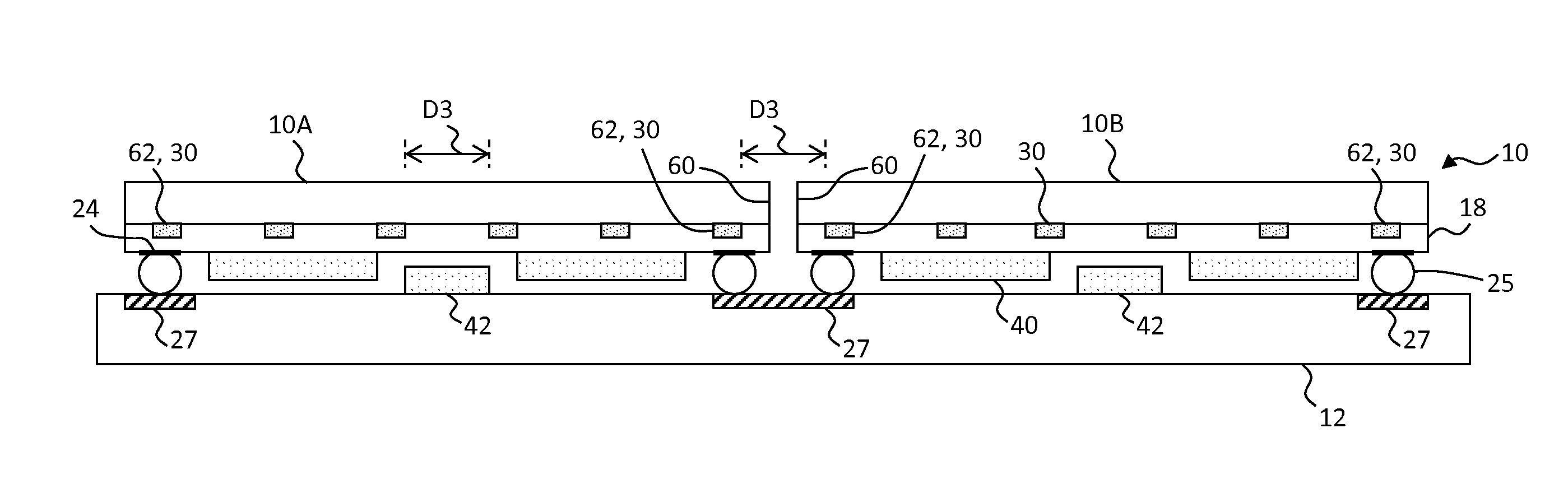
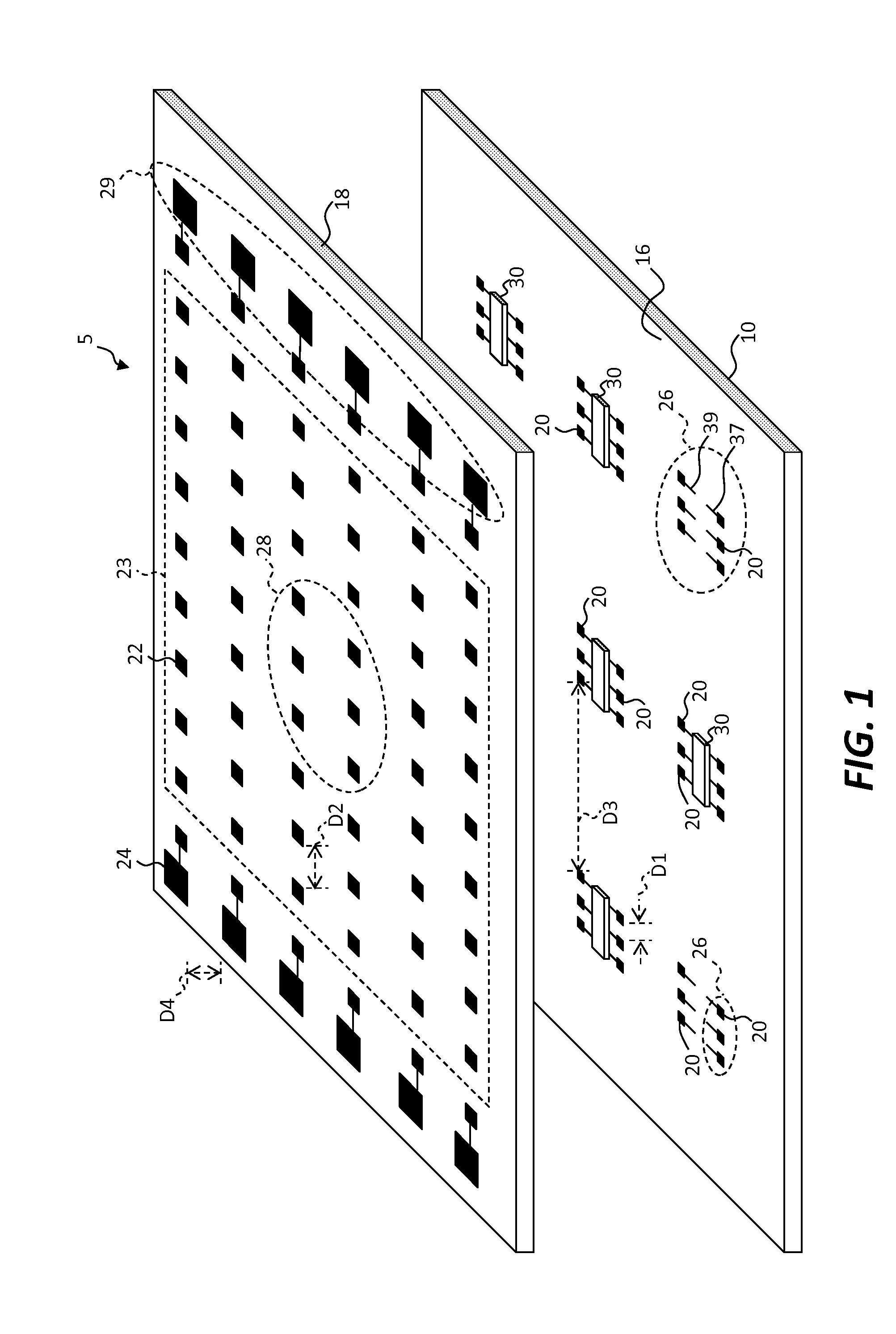
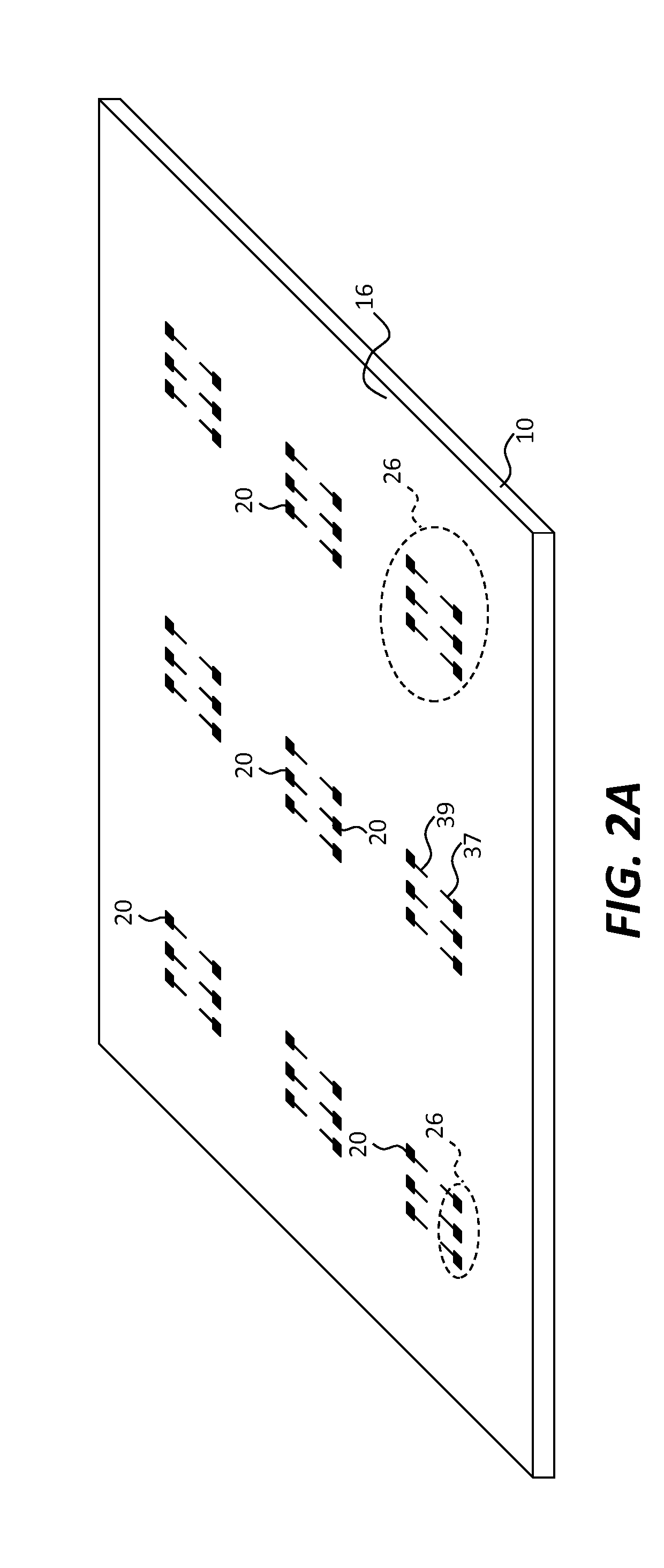
[0073]Referring to the exploded perspective of FIG. 1 and the partial details of FIGS. 2A and 2B, in an embodiment of the present invention a structure with an interconnection layer 5 for the redistribution of electrical connections includes a substrate 10 having a plurality of first electrical connections 20 disposed on a substrate surface 16 of the substrate 10 in a first arrangement 26. An insulating layer 18 is disposed on the substrate 10 over the first electrical connections 20. In various embodiments, the insulating layer 18 is light absorbing, is a black matrix, includes light-absorbing dyes or pigments, or is black. A plurality of second electrical connections 22 is disposed on the insulating layer 18 in a second arrangement 28 and disposed on a side of the insulating layer 18 opposite the plurality of first electrical connections 20. The second electrical connections 22 can be arranged in an array 23, for example a regular array 23.
[0074]The first and second electrical con...
PUM
 Abstract
Description
Claims
Application Information