Stage circuit and scan driver using the same

a technology of stage circuit and scan driver, which is applied in the direction of static storage, digital storage, instruments, etc., can solve the problems of increasing the consumption of such display devices as a liquid crystal display device (lcd), an organic light emitting display device (oled), and a plasma display panel (pdp). , to achieve the effect of improving reliability, reducing or reducing the rise of voltage, and increasing the falling time of a node q voltag

Active Publication Date: 2017-02-02
SAMSUNG DISPLAY CO LTD
View PDF11 Cites 5 Cited by
  • Summary
  • Abstract
  • Description
  • Claims
  • Application Information

AI Technical Summary

Benefits of technology

[0010]Embodiments of the present invention are directed toward a stage circuit and a scan driver using the same, capable of reducing or minimizing mounting area.
[0023]The stage circuit and the scan driver using the same in accordance with an embodiment of the present invention may increase a falling time of a voltage of a node Q and, at the same time, minimize or reduce a rise in voltage. If the falling time of the voltage of the node Q increases, the voltage of the output terminal may fall rapidly, and accordingly reliability may be improved and, at the same time, mounting area of the transistor coupled to the output terminal may be reduced or minimized. Furthermore, if a voltage increase of the node Q is lowered, stress on the transistor coupled to the node Q may be reduced and, at the same time, mounting area may be reduced or minimized.

Problems solved by technology

Reflecting such trend, consumption of such display devices as a liquid crystal display device (LCD), an organic light emitting display device (OLED), and a plasma display panel (PDP), is increasing.

Method used


Image

  • Stage circuit and scan driver using the same
  • Stage circuit and scan driver using the same
  • Stage circuit and scan driver using the same

Examples


Embodiment Construction

[0034]In the following detailed description, only certain exemplary embodiments of the present invention have been shown and described, simply by way of illustration. As those skilled in the art would realize, the described embodiments may be modified in various different ways, all without departing from the spirit or scope of the present invention. Accordingly, the drawings and description are to be regarded as illustrative in nature and not restrictive.

[0035]Unless otherwise defined, all terms (including technical and scientific terms) used herein have the same meaning as commonly understood by one of ordinary skill in the art to which this invention belongs. It will be further understood that terms, such as those defined in commonly used dictionaries, should be interpreted as having a meaning that is consistent with their meaning in the context of the relevant art and will not be interpreted in an idealized or overly formal sense unless expressly so defined herein.
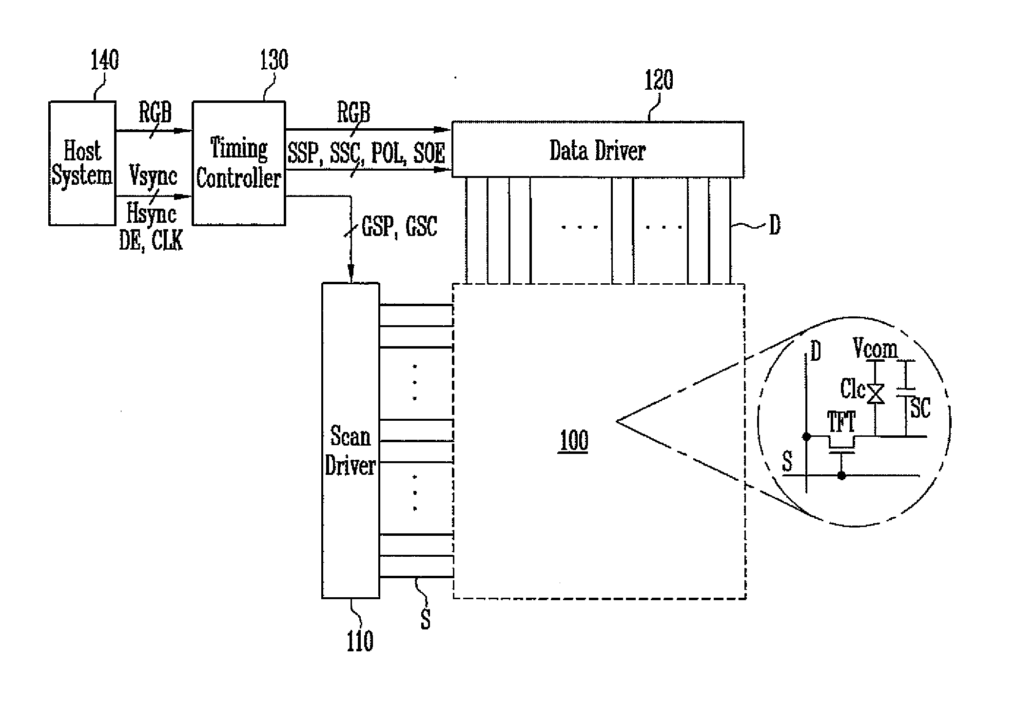
[0036]FIG. 1 is...


PUM


Abstract

A stage circuit includes an output part configured to supply a carry signal to a first output terminal and a scan signal to a second output terminal, in response to a voltage of a first node, a voltage of a second node, and a first clock signal being supplied to a first input terminal, a controller configured to control the voltage of the second node in response to the first clock signal being supplied to the first input terminal, a pull-up part configured to control the voltage of the first node in response to a carry signal of a previous stage being supplied to a second input terminal, and a pull-down part configured to control the voltage of the first node in response to the voltage of the second node and the carry signal of a next stage being supplied to a third input terminal.

Description

CROSS-REFERENCE TO RELATED APPLICATION[0001]This application claims priority to and the benefit of Korean Patent Application No. 10-2015-0106678, filed on Jul. 28, 2015, in the Korean Intellectual Property Office, the entire content of which is incorporated herein by reference in its entirety.BACKGROUND[0002]1. Field[0003]Aspects of embodiments of the present invention relate to a stage circuit and a scan driver using the same.[0004]2. Description of the Related Art[0005]As information technology advances, the importance of a display device, which is a medium between information and its user, is becoming more and more important. Reflecting such trend, consumption of such display devices as a liquid crystal display device (LCD), an organic light emitting display device (OLED), and a plasma display panel (PDP), is increasing.[0006]Generally, a display device includes a data driver to supply data signals to data lines, a scan driver to supply scan signals to scan lines, and a pixel par...

Claims


Application Information

Patent Timeline
Patent Type & Authority Applications(United States)
IPC IPC(8): G09G3/36G11C19/28
CPCG09G3/3677G11C19/28G09G2310/08G09G3/3648G09G3/3696G09G3/2077G09G3/3674G11C19/184
Inventor KIM, JONG HEELEECHAI, CHONG CHUL
Owner SAMSUNG DISPLAY CO LTD
Why Eureka
Try Eureka