High productivity pecvd tool for wafer processing of semiconductor manufacturing

Inactive Publication Date: 2017-04-27
APPLIED MATERIALS INC
View PDF6 Cites 9 Cited by
  • Summary
  • Abstract
  • Description
  • Claims
  • Application Information

AI Technical Summary

Benefits of technology

The present patent relates to a cluster tool for processing semiconductor substrates. The cluster tool includes multiple process chambers that can simultaneously process four or more substrates. Each process chamber has a substrate support for holding multiple substrates, a single showerhead, and a single radio frequency power source. The showerhead has gas passages that improve process uniformity. The technical effect of this invention is that it increases the efficiency and cost-effectiveness of semiconductor processing.

Problems solved by technology

Substrate throughput in semiconductor processing is always a challenge.
However, uniformity may become an issue when there is more than one substrate to be processed at once in a process chamber.

Method used


Image

  • High productivity pecvd tool for wafer processing of semiconductor manufacturing
  • High productivity pecvd tool for wafer processing of semiconductor manufacturing
  • High productivity pecvd tool for wafer processing of semiconductor manufacturing

Examples


Embodiment Construction

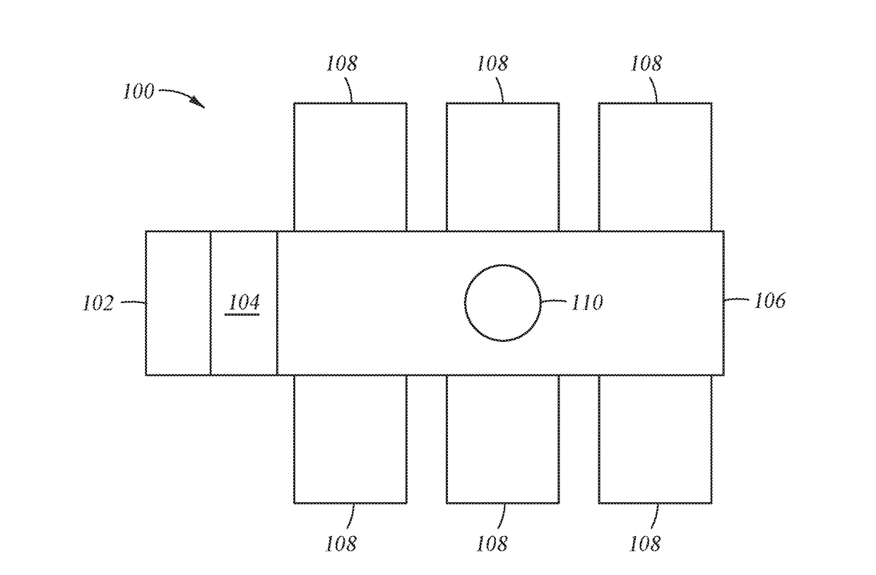
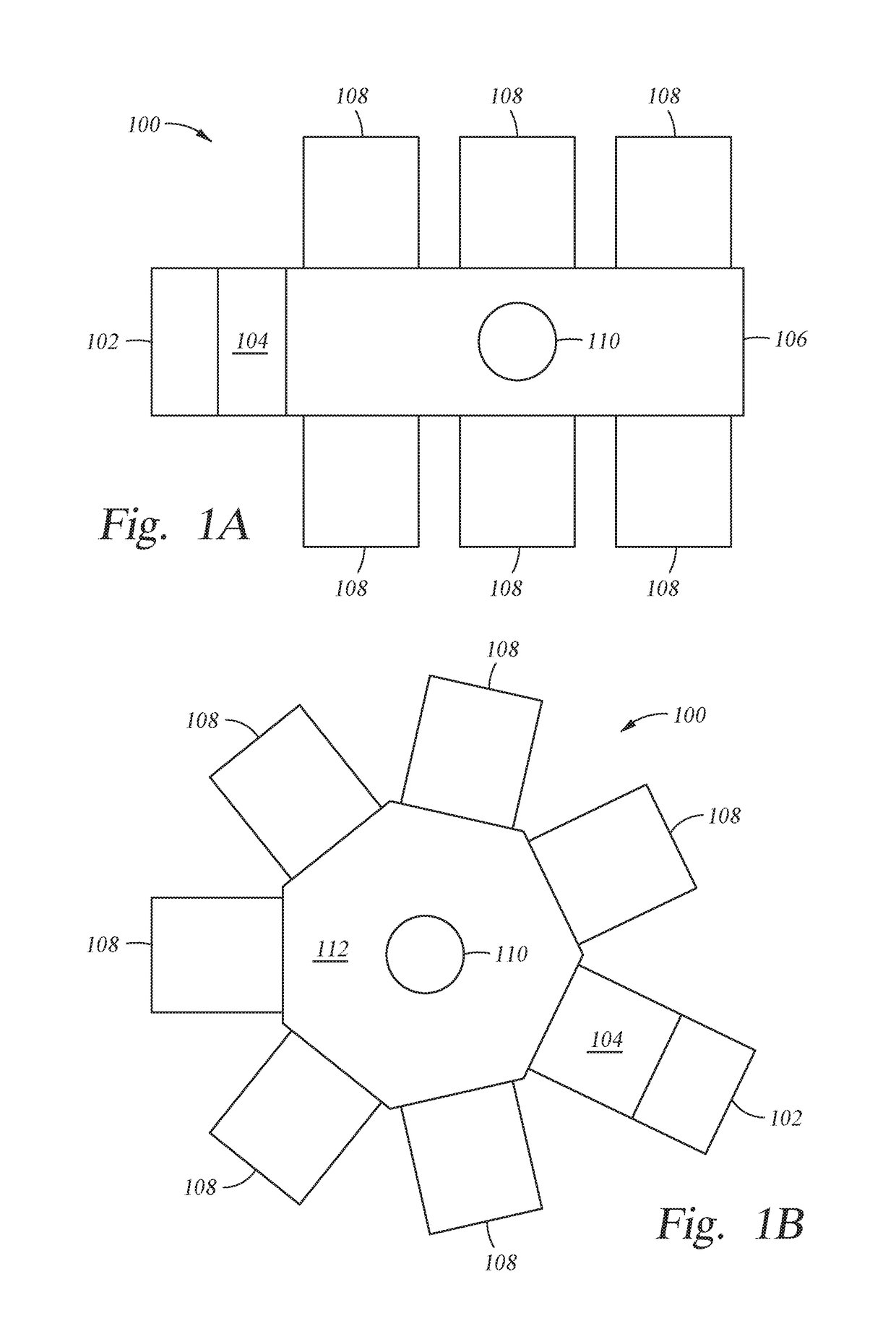
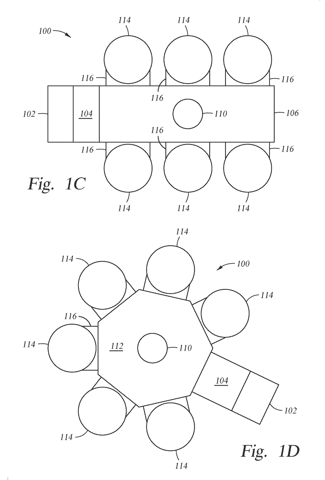
[0025]Embodiments of the present disclosure generally relate to a cluster tool for processing semiconductor substrates. In one embodiment, a cluster tool includes a plurality of process chambers connected to a transfer chamber and each process chamber may simultaneously process four or more substrates. In order to reduce cost, each process chamber includes a substrate support for supporting four or more substrates, single showerhead disposed over the substrate support, and a single radio frequency power source electrically coupled to the showerhead. The showerhead may include a first surface facing the substrate support and a second surface opposite the first surface. A plurality of gas passages may be formed in the showerhead extending from the first surface to the second surface. Process uniformity is improved by increasing the density of the gas passages from the center of the showerhead to the edge of the showerhead.

[0026]FIGS. 1A-1D schematically illustrate a cluster tool 100 a...


PUM

PropertyMeasurementUnit
Densityaaaaaaaaaa
Flexibilityaaaaaaaaaa
Frequencyaaaaaaaaaa

Abstract

Embodiments of the present disclosure generally relate to a cluster tool for processing semiconductor substrates. In one embodiment, a cluster tool includes a plurality of process chambers connected to a transfer chamber and each process chamber may simultaneously process four or more substrates. In order to reduce cost, each process chamber includes a substrate support for supporting four or more substrates, single showerhead disposed over the substrate support, and a single radio frequency power source electrically coupled to the showerhead. The showerhead may include a first surface facing the substrate support and a second surface opposite the first surface. A plurality of gas passages may be formed in the showerhead extending from the first surface to the second surface. Process uniformity is improved by increasing the density of the gas passages from the center of the showerhead to the edge of the showerhead.

Description

CROSS-REFERENCE TO RELATED APPLICATIONS[0001]This application claims priority to U.S. Provisional Patent Application Ser. No. 62 / 246,292, filed on Oct. 26, 2015 and U.S. Provisional Patent Application Ser. No. 62 / 277,719, filed on Jan. 12, 2016, which herein are incorporated by reference.BACKGROUND[0002]Field[0003]Embodiments of the present disclosure generally relate to a cluster tool for processing semiconductor substrates.[0004]Description of the Related Art[0005]Substrate throughput in semiconductor processing is always a challenge. If technology is to advance, semiconductor substrates continually need to be processed efficiently. Cluster tools have developed as an effective means for processing multiple substrates simultaneously without breaking vacuum. Instead of processing a single substrate and then exposing the substrate to atmosphere during transfer to another chamber, multiple process chambers can be connected to a common transfer chamber so that when a process is complet...

Claims


Application Information

Patent Timeline
IPC IPC(8): C23C16/455C23C16/50C23C16/458H01L21/67
CPCC23C16/45565H01L21/67196C23C16/458H01L21/67161C23C16/50H01L21/67201C23C16/5096H01J37/32899H01L21/6719H01L21/02274H01L21/67739H01L21/6835
Inventor ZHANG, LINLU, XUESONGLE, ANDREW V.YUAN, ZHENGOH, JANG SEOKFARAH, JOSEPH JAMILWANG, RONGPING
Owner APPLIED MATERIALS INC
Why Eureka
Try Eureka