Vertical memory devices and methods of manufacturing the same

a technology of vertical memory and manufacturing methods, applied in the direction of semiconductor devices, semiconductor/solid-state device details, electrical apparatus, etc., can solve the problems that the structural and electrical reliability of vertical memory devices may not be easily achieved

Active Publication Date: 2017-04-27
SAMSUNG ELECTRONICS CO LTD
View PDF1 Cites 345 Cited by
  • Summary
  • Abstract
  • Description
  • Claims
  • Application Information

AI Technical Summary

Benefits of technology

[0010]In accordance with one or more other embodiments, a vertical memory device includes a substrate; a gate line stack structure on the substrate and including: gate lines stacked and spaced apart from each other in a first direction with respect to a surface of the substrate; insulating interlayer patterns stacked and spaced apart from each other by the gate lines in the first direction; and channels extending through the insulating interlayer patterns and the gate lines in the first direction; a first etch-stop layer on the gate line stack structure and including an insulation material; a second etch-stop layer on the first etch-stop layer and including a conductive material; and contacts extending through the second etch-stop layer and the first etch-stop layer and electrically connected to the gate lines. The insulating interlayer patterns and the gate lines may be alternately stacked along the first direction in a stepped shape, the insulating interlayer patterns and gate lines may include step portions protruding in a second direction, and step portions of the gate lines may be covered by step portions of the insulating interlayer p

Problems solved by technology

Thus, structural and electrical reliability of the

Method used


Image

  • Vertical memory devices and methods of manufacturing the same
  • Vertical memory devices and methods of manufacturing the same
  • Vertical memory devices and methods of manufacturing the same

Examples


Embodiment Construction

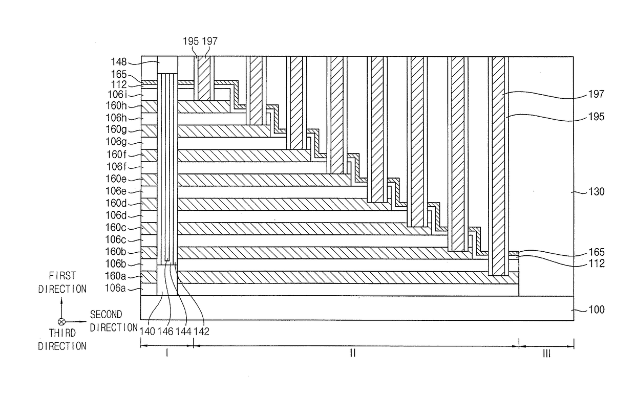
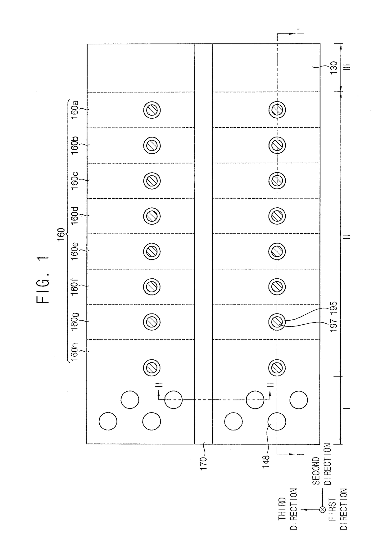
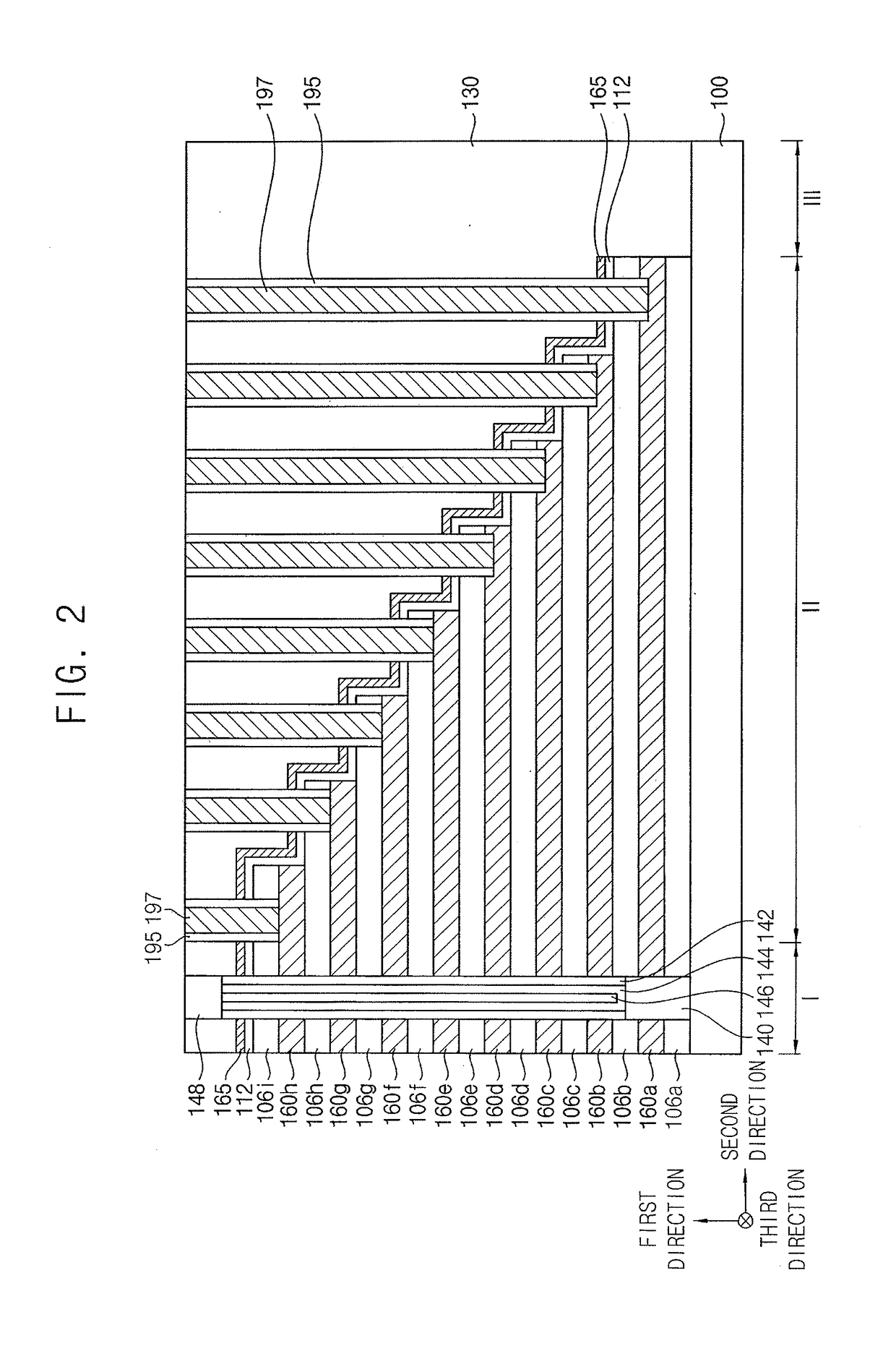
[0022]Example embodiments will now be described more fully hereinafter with reference to the accompanying drawings; however, they may be embodied in different forms and should not be construed as limited to the embodiments set forth herein. Rather, these embodiments are provided so that this disclosure will be thorough and complete, and will fully convey exemplary implementations to those skilled in the art. The embodiments may be combined to form additional embodiments.

[0023]In the drawings, the dimensions of layers and regions may be exaggerated for clarity of illustration. It will also be understood that when a layer or element is referred to as being “on” another layer or substrate, it can be directly on the other layer or substrate, or intervening layers may also be present. Further, it will be understood that when a layer is referred to as being “under” another layer, it can be directly under, and one or more intervening layers may also be present. In addition, it will also be...


PUM


Abstract

A vertical memory device includes a plurality of gate lines, at least one etch-stop layer, channels, and contacts. The gate lines are stacked and spaced apart from each other along a first direction with respect to a surface of substrate. Each of the gate lines includes step portion protruding in a second direction. The at least one etch-stop layer covers the step portion of at least one of the gate lines and includes conductive material. The channels extend through the gate lines in the first direction. The contacts extend through the at least one etch-stop layer and are on the step portions of the gate lines.

Description

CROSS-REFERENCE TO RELATED APPLICATION[0001]Korean Patent Application No. 10-2015-0147061, filed on Oct. 22, 2015, and entitled, “Vertical Memory Devices and Methods of Manufacturing the Same,” is incorporated by reference herein in its entirety.BACKGROUND[0002]1. Field[0003]One or more embodiments described herein relate to vertical memory devices and methods for manufacturing vertical memory devices.[0004]2. Description of the Related Art[0005]A vertical memory device has been developed having a relatively high degree of integration. Such a memory device includes memory cells stacked vertically with respect to the surface of a substrate. A channel having a pillar or cylindrical shape protrudes vertically from the substrate surface, and gate lines and insulation layers surrounding the channel are repeatedly stacked.[0006]As the degree of integration of the vertical memory device increases, the numbers of the gate lines and insulation layers increase. Thus, structural and electrical...

Claims


Application Information

Patent Timeline
IPC IPC(8): H01L23/528H01L23/522H01L21/768H01L27/115
CPCH01L23/5283H01L27/1157H01L27/11582H01L27/11573H01L21/76816H01L21/76829H01L21/76877H01L23/5226H01L21/76831H01L21/76832H01L21/76834H10B43/50H10B43/35H10B43/27H10B43/40
Inventor KIM, HYUKMIN, JAE-HOPARK, JONG-KYOUNGCHUNG, SEUNG-PIL
Owner SAMSUNG ELECTRONICS CO LTD
Why Eureka
Try Eureka