High speed high density electrical connector

a high-density, electrical connector technology, applied in the direction of connection of the connection contact member, contact member manufacturing, connection contact member material, etc., can solve the problems of increasing the possibility of energy loss, and reducing the efficiency of electrical connections, so as to reduce or eliminate electrical noise

Active Publication Date: 2007-01-16
AMPHENOL CORP
View PDF4 Cites 335 Cited by
  • Summary
  • Abstract
  • Description
  • Claims
  • Application Information

AI Technical Summary

Benefits of technology

[0014]In one aspect, the invention relates to a wafer for an electrical connector having a plurality of wafers. The wafer includes a housing comprising a first, insulative housing and a second, conductive housing. The wafer also includes a plurality of signal strips disposed within the first, insulative housing. The first, insulative housing includes an insulative material securing the plurality of signal strips and spacing the plurality of signal strips from the second, conductive housing. The second, conductive housing is formed of a non-conductive binder material having conductive particles disposed therein thereby rendering the second, conductive housing conductive. The second, conductive housing is configured and arranged relative to the plurality of signal strips to shield at least some of the plurality of signal strips to reduce or eliminate electrical noise, with the wafer being free of a metal shield plate.
[0015]In another aspect, the invention relates to a wafer for an electrical connector having a plurality of wafers. The wafer includes a housing comprising a first, insulative housing and a second, conductive housing. The wafer also includes a plurality of signal strips disposed within the first, insulative housing. The first, insulative housing includes an insulative material securing the plurality of signal strips and spacing the plurality of signal strips from the second, conductive housing. At least one ground strip is disposed within and electrically coupled to the second, conductive housing. The at least one ground strip is disposed in a plane and the plurality of signal strips is disposed in the same plane. The second, conductive housing is formed of a non-conductive binder material having conductive particles disposed therein thereby rendering the second, conductive housing conductive. The second, conductive housing being configured and arranged relative to the plurality of signal strips to shield at least some of the plurality of signal strips to reduce or eliminate electrical noise.

Problems solved by technology

Electronic systems have generally become smaller, faster and functionally more complex.
As frequency content increases, there is a greater possibility of energy loss.
Energy loss can be attributed to impedance discontinuities, mode conversion, leakage from imperfect shielding, or undesired coupling to other conductors (crosstalk).

Method used


Image

  • High speed high density electrical connector
  • High speed high density electrical connector
  • High speed high density electrical connector

Examples


Embodiment Construction

[0024]This invention is not limited in its application to the details of construction and the arrangement of components set forth in the following description or illustrated in the drawings. The invention is capable of other embodiments and of being practiced or of being carried out in various ways. Also, the phraseology and terminology used herein is for the purpose of description and should not be regarded as limiting. The use of “including,”“comprising,” or “having,”“containing,”“involving,” and variations thereof herein, is meant to encompass the items listed thereafter and equivalents thereof as well as additional items.

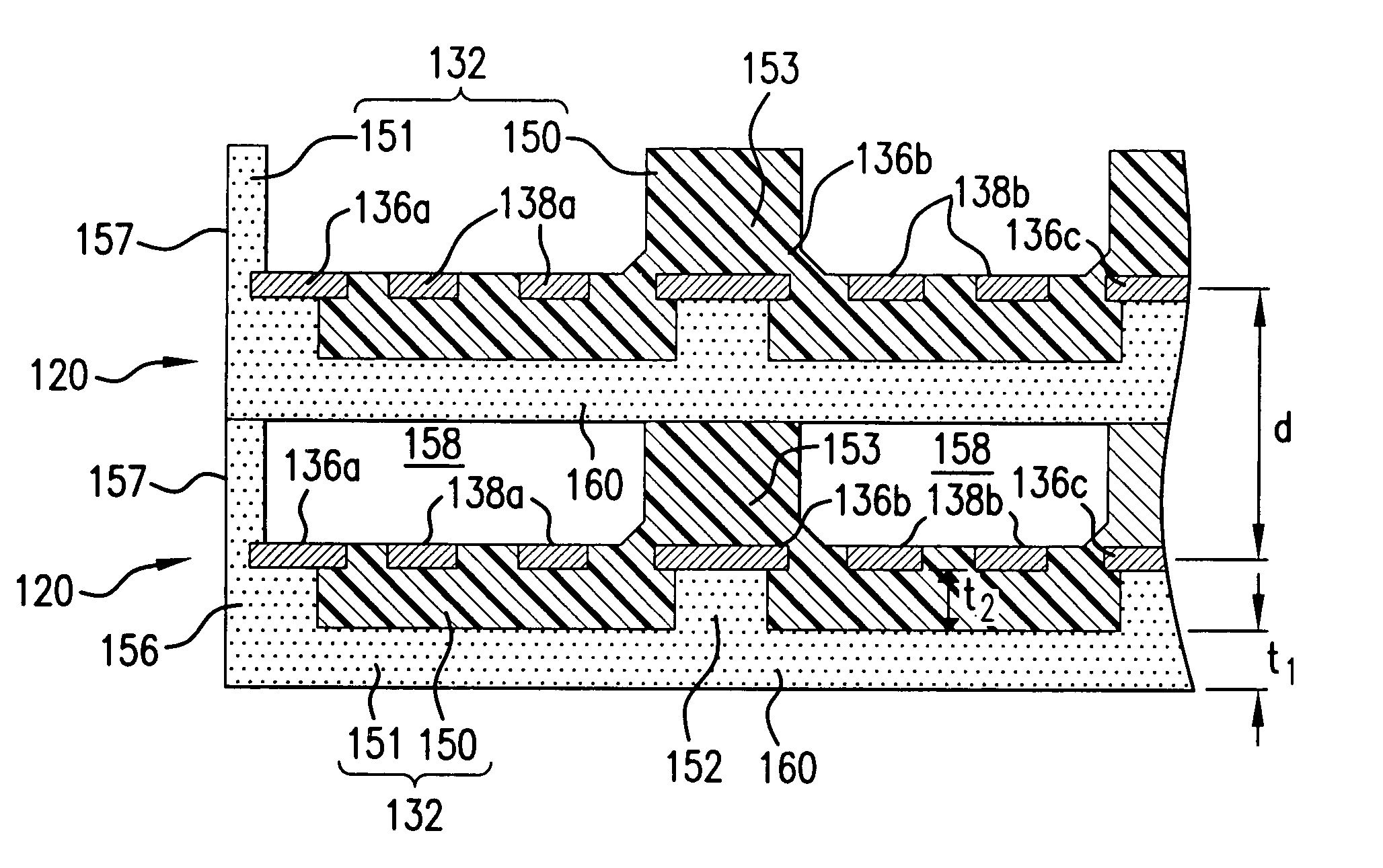
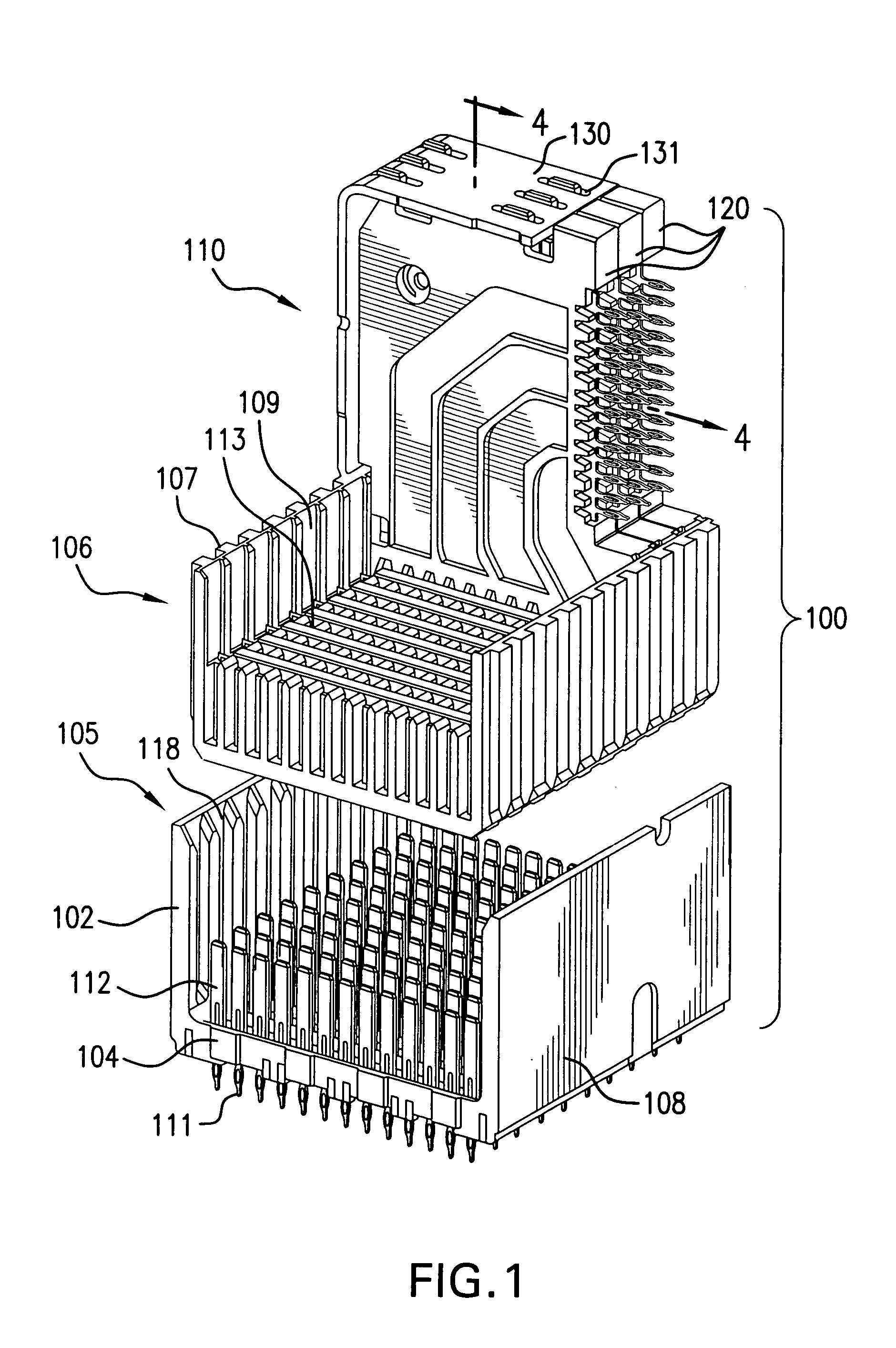
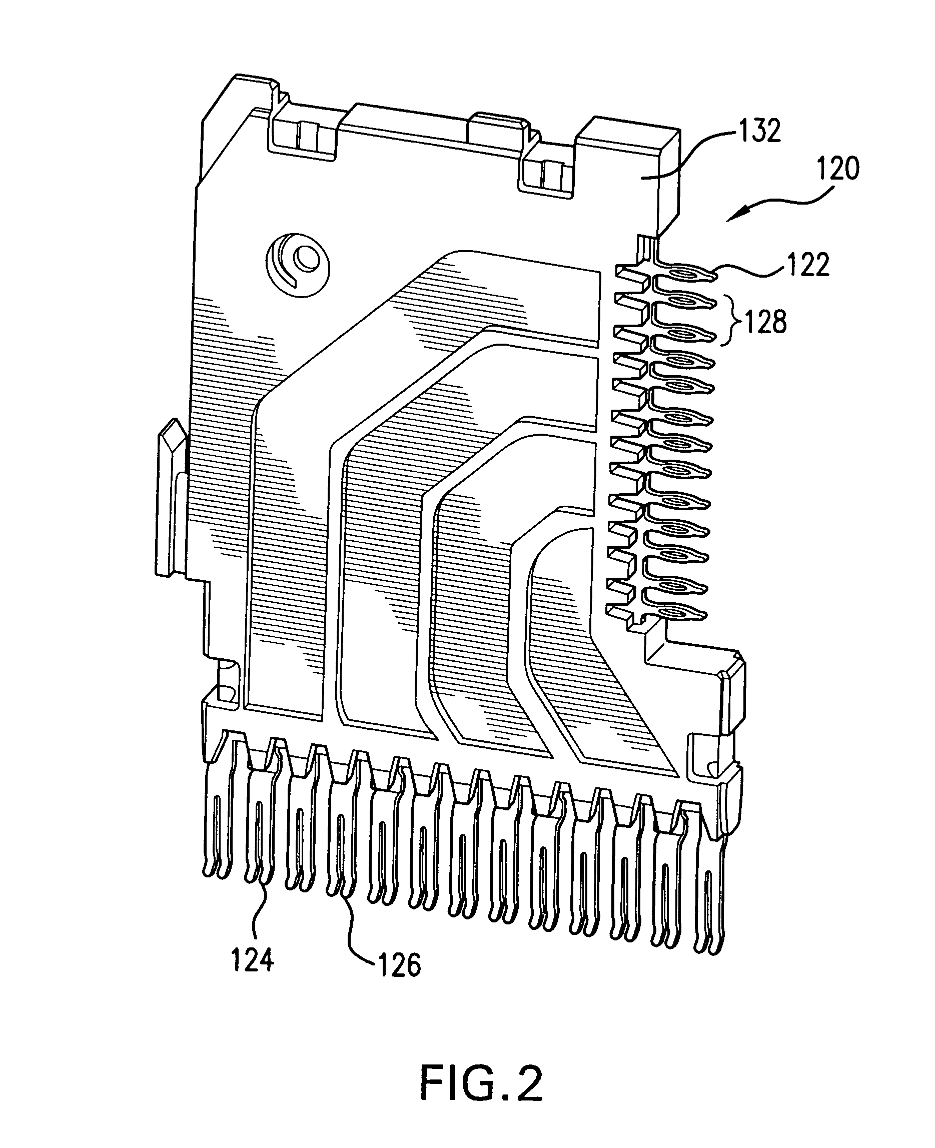
[0025]Conventional daughter board connectors are typically formed from a plurality of individual wafers coupled together. Each wafer includes a signal frame molded within a non-conductive housing. A metal ground shield plate and connected metal strips may be employed within the wafer to minimize electrical noise generated in the wafer in forms such as reflection...


PUM

PropertyMeasurementUnit
thicknessaaaaaaaaaa
distanceaaaaaaaaaa
distanceaaaaaaaaaa

Abstract

An electrical connector includes a wafer formed with a ground shield made from a non-conductive material made conductive with conductive particles disposed therein, thereby eliminating the necessity of the metal ground shield plate found in prior art connectors while maintaining sufficient performance characteristics and minimizing electrical noise generated in the wafer. The wafer housing is formed with a first, insulative housing at least partially surrounding a pair of signal strips and a second, conductive housing at least partially surrounding the first, insulative housing and the signal strips. The housings provide the wafer with sufficient structural integrity, obviating the need for additional support structures or components for a wafer. Ground strips may be employed in the wafer and may be formed in the same plane as the signal strips. The second, conductive housing may be connected (e.g., molded) to the ground strips and spaced appropriately from the signal strips. The wafer may also include air gaps between the signal strips of one wafer and the conductive housing of an adjacent wafer further reducing electrical noise or other losses (e.g., cross-talk) without sacrificing significant signal strength.

Description

RELATED APPLICATIONS[0001]This application claims the benefit of U.S. Provisional Patent Application Ser. No. 60 / 695,705, filed Jun. 30, 2005, entitled “High Speed, High Density Electrical Connector”, which is hereby incorporated herein by reference.BACKGROUND OF INVENTION[0002]1. Field of Invention[0003]This invention relates generally to electrical interconnection systems and more specifically to improved signal integrity in interconnection systems, particularly in high speed electrical connectors.[0004]2. Discussion of Related Art[0005]Electrical connectors are used in many electronic systems. It is generally easier and more cost effective to manufacture a system on several printed circuit boards (“PCBs”) which are then connected to one another by electrical connectors. A traditional arrangement for connecting several PCBs is to have one PCB serve as a backplane. Other PCBs, which are called daughter boards or daughter cards, are then connected through the backplane by electrical...

Claims


Application Information

Patent Timeline
Patent Type & Authority Patents(United States)
IPC IPC(8): H01R13/648H01R13/6461H01R13/6477H01R13/658H01R13/6586H01R13/6599
CPCH01R13/514H01R13/6587H01R23/688H01R23/7073H01R12/727H01R13/6599H01R12/585H01R12/724H01R13/516Y10T29/4922H01R43/16H01R43/24H01R13/6461
Inventor COHEN, THOMAS S.KIRK, BRIANCARTIER, JR., MARC B.
Owner AMPHENOL CORP
Why Eureka
Try Eureka