Sensor substrate and method of fabricating same

a technology of sensor substrate and substrate, which is applied in the field of sensor technology, can solve the problems of inconvenient blood drawing and insulin injection thousands of times, painful and emotionally debilitating, and invasiveness in the biosensing field

Inactive Publication Date: 2008-01-29
MEDTRONIC MIMIMED INC
View PDF81 Cites 338 Cited by
  • Summary
  • Abstract
  • Description
  • Claims
  • Application Information

AI Technical Summary

Benefits of technology

[0012]According to another embodiment of the present invention, a sensing apparatus may include a substrate having a first area for a sensing element and a second area for electronics. The sensing apparatus may also include one or more vias making electrical contact from the first area of the substrate to the second area of the substrate. The via may be hermetically sealed from the first area of the substrate to the second area of the substrate and may be filled with a conductive material.

Problems solved by technology

Nonetheless, challenges in the biosensing field have remained.
For example, although many diabetics currently utilize diagnostic medical equipment in the comfort of their own homes, the vast majority of such devices still require diabetics to draw their own blood and inject their own insulin.
Under any circumstances, drawing blood and injecting insulin thousands of times is invasive and inconvenient at best and most likely painful and emotionally debilitating.
Unfortunately, oxygen sensors implanted into the body have, thus far, typically required frequent and periodic checking and recalibration.
Up until now, such a sensor has been unavailable.
However, attempts to place sensor electronics in close proximity to the sensor in implantable sensor systems have historically suffered from the environment in which they operate.
This poses obvious dangers for the sensor electronics.
The sensor electronics must remain in electrical contact with the sensor; however, any exposure of the sensor electronics to the blood or any other fluid would potentially short circuit the sensor electronics and destroy the entire system.

Method used


Image

  • Sensor substrate and method of fabricating same
  • Sensor substrate and method of fabricating same
  • Sensor substrate and method of fabricating same

Examples


Embodiment Construction

[0042]In the following description of preferred embodiments, reference is made to the accompanying drawings which form a part hereof, and in which are shown by way of illustration specific embodiments in which the invention may be practiced. It is to be understood that other embodiments may be utilized and structural changes may be made without departing from the scope of the preferred embodiments of the present invention.

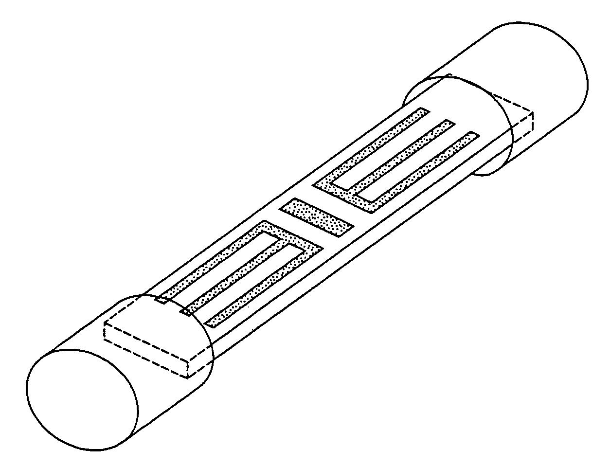
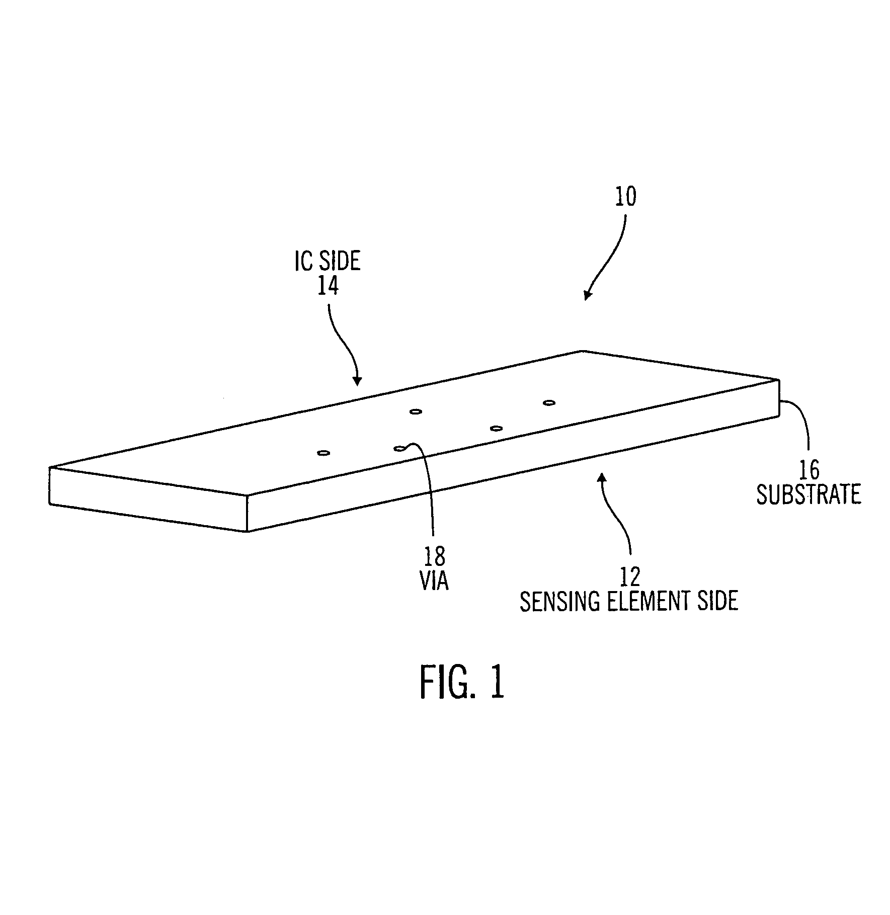
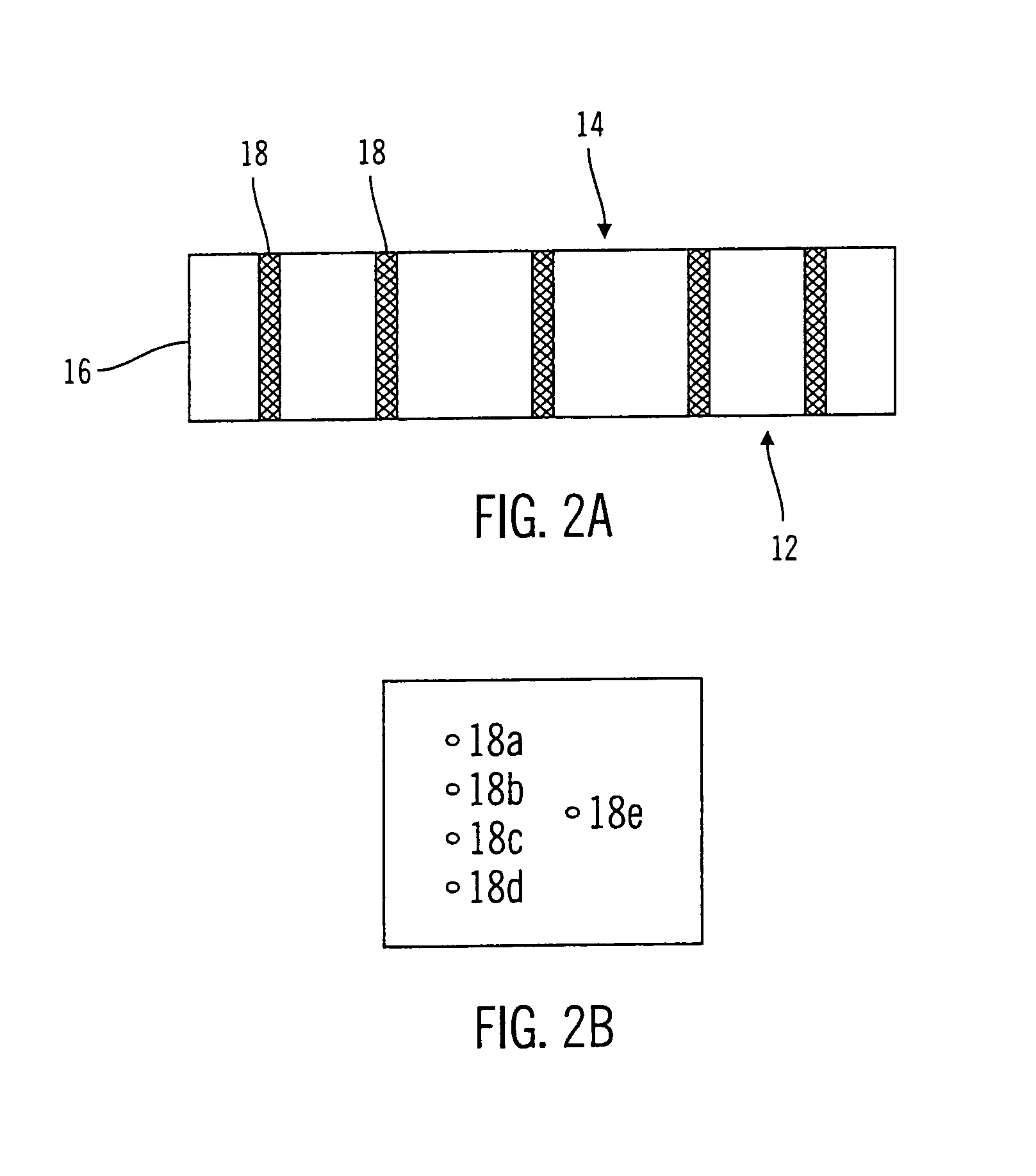
[0043]FIG. 1 shows a generalized substrate configuration according to an embodiment of the present invention. A sensor 10 has a sensing element side 12 of a substrate 16 on which a biosensing element, physiological parameter sensing element or other sensing element may be affixed. The sensor 10 also has an electronics side 14 of the substrate 16 on which electronics may be affixed for processing signals generated by the sensing element.

[0044]The sensing element side 12 may support any of a variety of sensing elements. For example, the sensing element may be a gluco...


PUM

PropertyMeasurementUnit
thicknessaaaaaaaaaa
thickaaaaaaaaaa
thicknessaaaaaaaaaa

Abstract

A substrate with hermetically sealed vias extending from one side of the substrate to another and a method for fabricating same. The vias may be filled with a conductive material such as, for example, a fritless ink. The conductive path formed by the conductive material aids in sealing one side of the substrate from another. One side of the substrate may include a sensing element and another side of the substrate may include sensing electronics.

Description

CROSS-REFERENCE TO RELATED APPLICATIONS[0001]Embodiments of the present invention claim priority from a U.S. Provisional Application entitled “Sensor Substrate and Method of Fabricating Same,” Ser. No. 60 / 318,055, filed Sep. 7, 2001, the contents of which are incorporated by reference herein.BACKGROUND[0002]1. Field of the Invention[0003]The present invention relates to the field of sensor technology and, in particular, to the formation of hermetically sealed substrates used for sensing a variety of parameters, including physiological parameters.[0004]2. Description of Related Art[0005]The combination of biosensors and microelectronics has resulted in the availability of portable diagnostic medical equipment that has improved the quality of life for countless people. Many people suffering from disease or disability who, in the past, were forced to make routine visits to a hospital or doctor's office for diagnostic testing currently perform diagnostic testing on themselves in the com...

Claims


Application Information

Patent Timeline
Patent Type & Authority Patents(United States)
IPC IPC(8): G01N27/06G01N33/66A61B5/00H05K1/03H05K3/28H05K3/40
CPCH05K3/28H05K3/4061A61B5/0006H05K1/0306H05K2201/0175H05K2201/0179H05K2203/308H05K2201/09472H05K2203/082H05K2203/085H05K2203/1147H05K2203/1476H05K2203/1572H05K2201/0317
Inventor PENDO, SHAUNSHAH, RAJIVCHERNOFF, EDWARD
Owner MEDTRONIC MIMIMED INC
Why Eureka
Try Eureka