Hermetic wafer scale integrated circuit structure

a technology of integrated circuits and hermetic wafers, applied in the direction of semiconductor devices, semiconductor/solid-state device details, electrical devices, etc., can solve the problems of glass cutting operation cost and scrapping of entire wafers

Inactive Publication Date: 2006-01-03
MICRO CHIP SCALE PACKAGING
View PDF12 Cites 118 Cited by
  • Summary
  • Abstract
  • Description
  • Claims
  • Application Information

AI Technical Summary

Benefits of technology

[0012]That is, the layer of noble metal covering the interface between the sheet of glass, the adhesive material and the semiconductor die, and which extends around the entire perimeter of each IC die formed as part of the wafer structure, creates a hermetic seal that prevents moisture and other environmental elements from reaching the surface of the semiconductor die in the package. Thus, the hermetic seal prevents the sensitive electrical circuitry on the surface of the semiconductor die from being exposed to environmental elements that could damage or destroy those electrical circuits. The hermetically sealed chip scale package of the present invention allows the use of this compact inexpensive packaging methodology in severe environmental conditions.

Problems solved by technology

The disadvantages are that the extension of the connectors to the pads on the wafer are difficult to implement and often prevent the process from being possible, the glass cutting operation is costly and requires special equipment, the process is implemented on a completed semiconductor wafer which is very sensitive and costly and any error causes the entire wafer to be scrapped, and two sheets of glass are always required.

Method used


Image

  • Hermetic wafer scale integrated circuit structure
  • Hermetic wafer scale integrated circuit structure
  • Hermetic wafer scale integrated circuit structure

Examples


Embodiment Construction

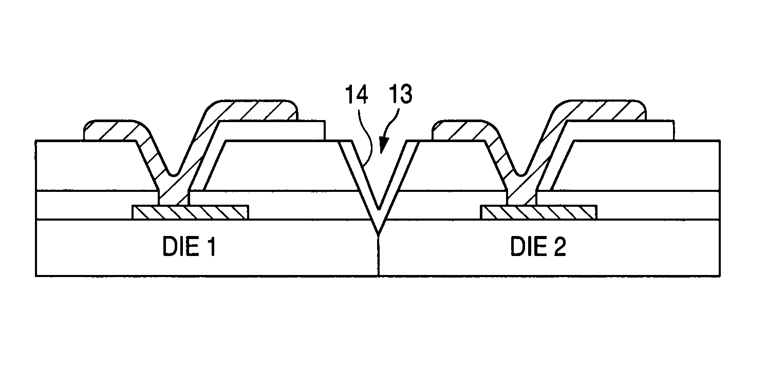
[0036]The following detailed description presents one method of manufacturing a wafer scale structure of hermetically sealed semiconductor integrated circuit dies in accordance with the present invention.

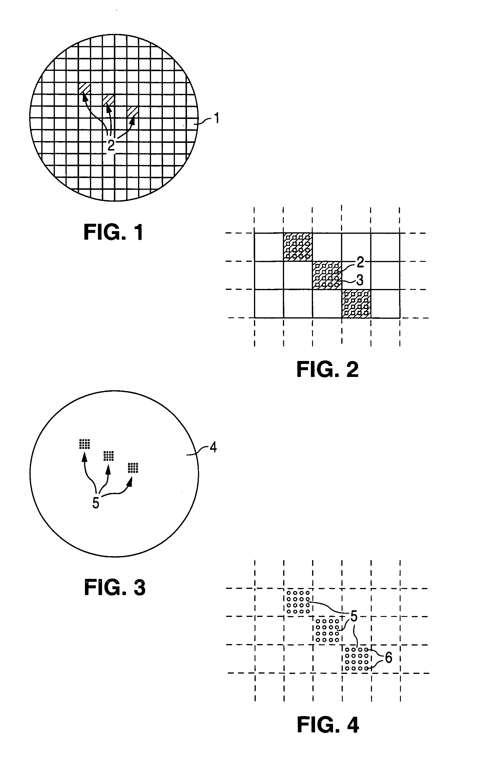
[0037]Manufacture of the wafer scale structure begins with a semiconductor wafer 1 as shown in FIG. 1. On the semiconductor wafer 1 are formed a number of individual semiconductor integrated circuit die 2. The principle of the present invention can be applied to any size semiconductor wafer, including 4-inch wafers, 6-inch wafers, 8-inch wafers and (when they become available) 12-inch wafers. Further, the invention is scalable beyond 12 inches and into any size wafer that can be created. The semiconductor wafer 1 can be created from any well-known semiconductor material including silicon, gallium arsenate and sapphire, although one of ordinary skill in the art will appreciate that any semiconductor material can be used.

[0038]FIG. 2 shows a close up view of individual integrated circ...


PUM


Abstract

A wafer scale semiconductor integrated circuit packaging technique provides a hermetic seal for the individual integrated circuit die formed as part of the wafer scale structure. A semiconductor wafer is manufactured to include a number of individual semiconductor die. Each individual die formed on the wafer includes a number of bond pads that are exposed on the die surface in various locations to provide electrical connections to the circuitry created on the die. The wafer further includes a planar glass sheet that is substantially the same size as the wafer, the glass sheet being adhered to the wafer using a suitable adhesive. The glass sheet has a number of pre-formed holes in it, the arrangement of the pre-formed holes corresponding to the location of the bond pads at each of the individual semiconductor die formed as part of the wafer structure. Following adherence of the glass sheet to the semiconductor wafer utilizing the intermediate adhesive material, metal connections are made between pads formed on the glass sheet and the bond pads formed on the integrated circuit die. Solder balls are then attached to the pads on the glass sheet to provide a conductive flow between the solder balls and the bond pads. After the solder balls are attached, trenches are cut around each of the individual die on the wafer. The trenches are cut at an angle and extend through the glass sheet and the intermediate adhesive material and into the semiconductor substrate in which the integrated circuits are formed. After the trenches are cut around each individual semiconductor die, a noble metal is deposited on the sidewalls of the trench to extend over the interface between the glass sheet, the adhesive material and the semiconductor die. The wafer is then cut along the noble metal lined trenches to provide individual, hermetically sealed packaged integrated circuit die.

Description

RELATED APPLICATION[0001]The present application is a Continuation-In-Part of co-pending U.S. application Ser. No. 09 / 045,507, filed Mar. 20, 1998, titled “CHIP SCALE PACKAGES” and of co-pending U.S. application Ser. No. 09 / 686,016, filed Oct. 10, 2000, titled “CHIP SCALE PACKAGES,” which is a divisional of application Ser. No. 09 / 045,507. Both application Ser. No. 09 / 045,507 and application Ser. No. 09 / 686,016 are hereby incorporated by reference in their entirety (application Ser. No. 09 / 686,016 is the subject of a Notice of Allowance issued by the U.S. Patent Office on May 21, 2002.).BACKGROUND OF THE INVENTION[0002]1. Field of the Invention[0003]The present invention relates generally to the packaging of semiconductor integrated circuit (IC) die and, in particular, to the packaging of semiconductor IC die in chip scale packages at the wafer level structure of the integrated circuit manufacturing process. In one of its aspects, the invention specifically relates to packaging indi...

Claims


Application Information

Patent Timeline
Patent Type & Authority Patents(United States)
IPC IPC(8): H01L23/12H01L21/60H01L23/31H01L23/485
CPCH01L23/3114H01L24/12H01L24/11H01L2224/0401H01L2224/0231H01L2224/13099H01L2924/01009H01L2924/01013H01L2924/01027H01L2924/01029H01L2924/01039H01L2924/01079H01L2924/01082H01L2924/14H01L2924/3011H01L2924/01006H01L2924/01023H01L2924/01024H01L2924/01033H01L2924/014H01L2224/04105H01L2224/05124H01L2224/05624H01L2224/05155H01L2224/05644H01L24/83H01L24/82H01L24/92H01L24/73H01L24/24H01L24/32H01L24/29H01L2224/3207H01L2224/8385H01L2224/83931H01L2224/82106H01L2224/92144H01L2224/73217H01L2224/24225H01L2224/244H01L2224/04073H01L2224/02H01L24/02H01L24/05H01L24/13H01L2224/05548H01L2224/13024H01L2224/13022H01L2224/0235H01L2224/02331H01L2224/02379H01L2224/24H01L2924/00014H01L2224/023H01L2924/0001H01L2924/00012H01L2224/02371
Inventor MACINTYRE, DONALD M.
Owner MICRO CHIP SCALE PACKAGING
Why Eureka
Try Eureka