[0014]Specifically, the invention relates to the production of thin films of bulk-quality
gallium nitride on synthetic diamond substrates wherein synthetic diamond is grown by
chemical vapor deposition method. The thin films of bulk-quality
gallium nitride may be “peeled” from commercially available bulk
gallium nitride wafers, but may also be “peeled” directly from bulk
gallium nitride boules to reduce kerf loss.
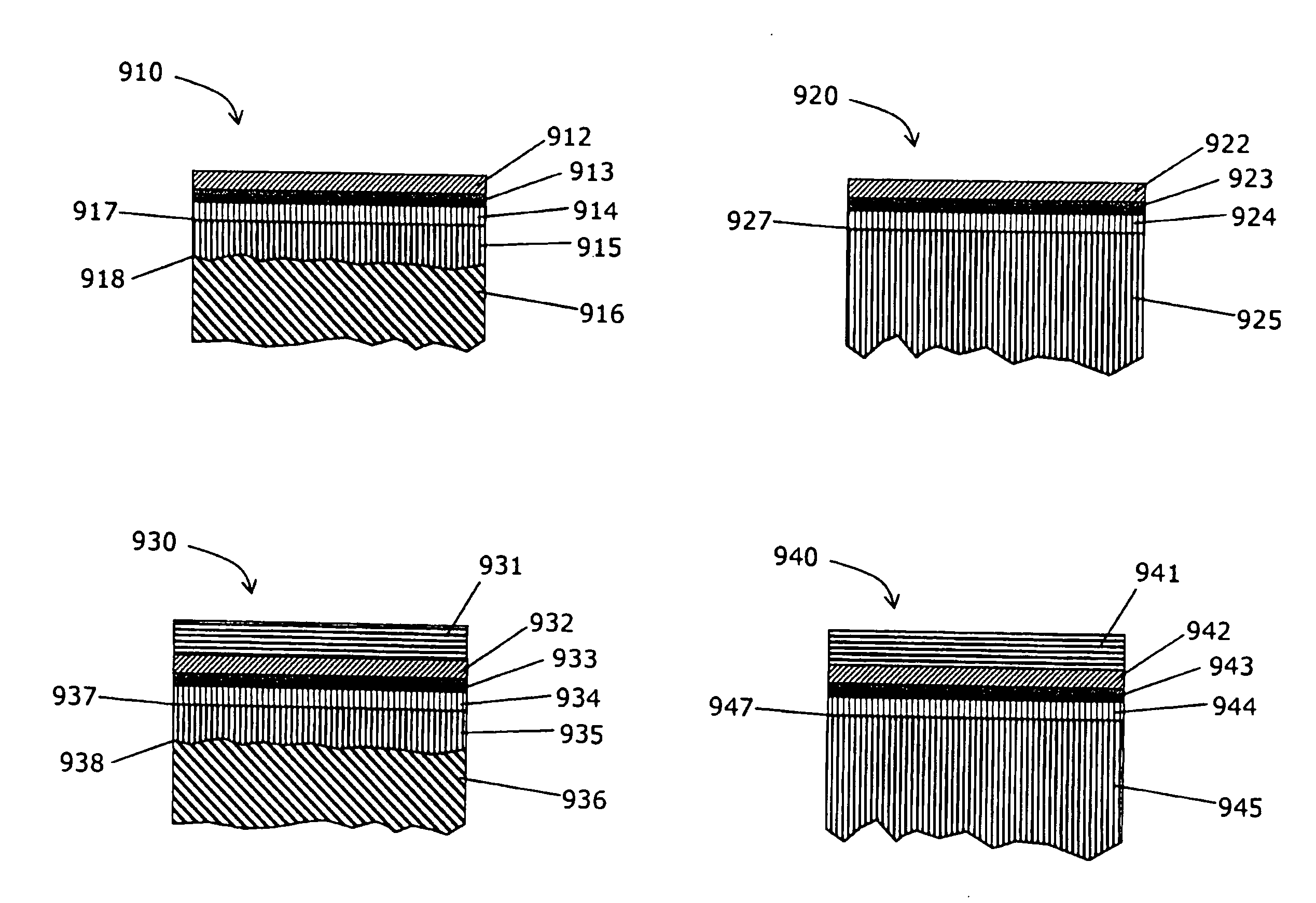
[0019]The invented process comprises atomically attaching a synthetic diamond layer or
layers to the surface of bulk GaN wafer that has been specially prepared by
ion implantation and then “peeling” off a
thin layer of bulk-quality GaN that is adjacent to the synthetic diamond layer(s) from the bulk GaN wafer. The remaining bulk GaN substrate, after suitable cleaning and
polishing, can be reused to peel another layer off the surface. In this way almost all of the bulk-grown GaN in the substrate is being used for growth and creation of high-performance devices, resulting substantially lower cost per device wafer and substantially higher quality GaN films available for device manufacturing that conventional methods in which GaN is grown on lattice-mismatched substrates (eg.
sapphire and
silicon).
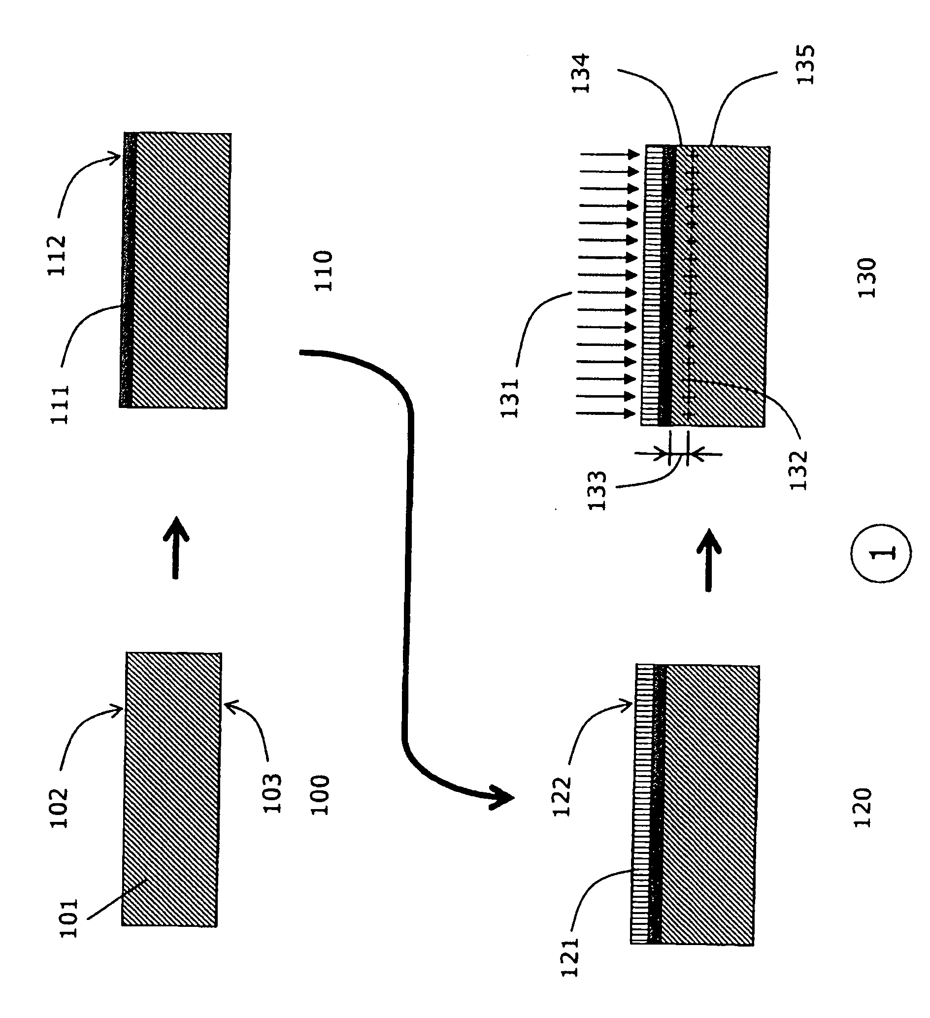
Synthetic Diamond[0027]In one embodiment of the present invention, the surface of the
gallium nitride is coated prior to the implantation and before the deposition of diamond
layers. The reasons are the following: The subsequent steps involve processes at elevated temperatures (in excess of 600° C.). The
decomposition of the GaN surface begins at temperatures above 600° C. with significant loss occurring around 900° C., and can be prevented by depositing a suitable
surface coating. Also, the
coating of GaN prevents the
decomposition of the gallium nitride surface during long and high-
dose implants [8]. This is especially true if the
implant is carried out at an elevated substrate temperature. Finally, the synthetic
diamond deposition requires a
surface preparation to efficiently nucleate. This is most easily realized by
coating the surface with a suitable amorphous material, such as,
silicon nitride. In one embodiment, the GaN is coated with at least one nucleating layer. In another embodiment, the
coating prior to implantation comprises a
silicon nitride layer followed by a synthetic diamond layer.
[0030]In one embodiment, a thin initial layer of synthetic diamond is grown prior to the implantation and then a stiffening layer and then a bulk layer of diamond are grown after the implantation. The diamond growth is nucleated prior to the implantation under conditions that facilitate quality
nucleation and initial rigidity of the diamond film. The initial diamond layer can be as thin as several nanometers, but its stability improves with the thickness hence thicknesses of several micrometers are possible.
Diamond thickness of 150 nm was used to simulate the
hydrogen implantation profile for this embodiment in FIG. 5. The conditions for growth of the diamond stiffener layer are adjusted so that the temperature does not
impact the implanted species or the detachment of the gallium nitride film. This means keeping the temperature below 600° C. and a low growth rate. The thickness of the diamond stiffener layer is determined by the desired rigidity of the diamond layer prior to raising the temperature for high growth rate step: the stiffener layer may be several micrometers thick. The conditions for growing the bulk diamond layer are optimized for high growth rate and consequently higher temperature (above 600° C.). The majority of the diamond layer (the “bulk” of the new substrate) is grown during this stage.
[0032]In another embodiment, the synthetic diamond growth commences with the stiffener diamond layer after the implantation at a temperature and method that sustains the stability of the thin GaN film. This means growing a low-temperature diamond (<600 C) for at least some of the
growth time, and then raising the temperature to a higher growth rate to grow the bulk diamond layer. For example,
microwave plasma is used at low temperature to growth the first one or more micrometers of the diamond (“stiffener diamond layer”) and then a different method and / or higher temperature is used to increase the growth rate during the later stage (“bulk diamond layer”).

