Display device

a display device and display technology, applied in the field of display devices, can solve the problems of deteriorating the touch function, unsatisfactory satisfaction of unintended interference, and needing to consider the interference between the touch sensor and the other components, and achieves the effect of reducing the level of external light reflection, facilitating application, and satisfactory optical characteristics and electrical characteristics

Active Publication Date: 2017-05-04
LG DISPLAY CO LTD
View PDF12 Cites 14 Cited by
  • Summary
  • Abstract
  • Description
  • Claims
  • Application Information

AI Technical Summary

Benefits of technology

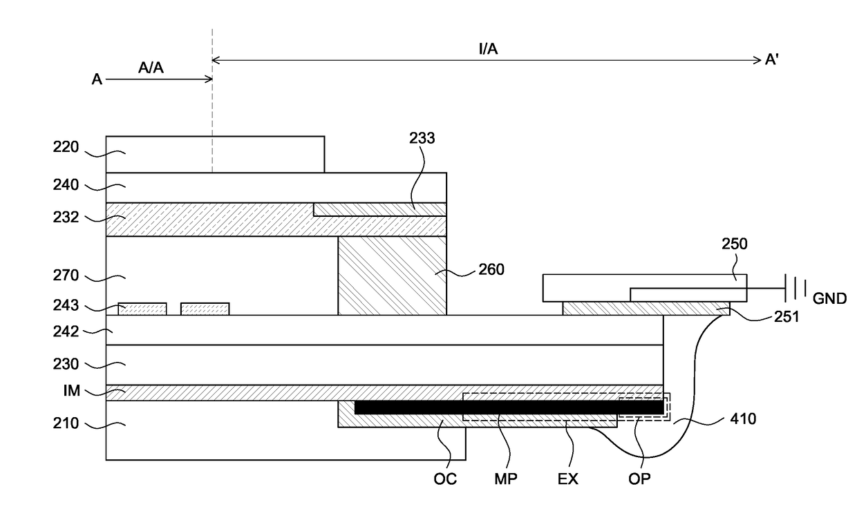
[0015]Still another object to be achieved by an embodiment of the present disclosure is to provide a display device in which a conductive layer functioning as a secondary sensor or facing sensor of a pressure-sensitive touch sensor is disposed between an in-cell capacitive touch sensor and the pressure-sensitive touch sensor. Thus, a touch sensor can be applied more easily and rapidly to the conductive layer through a metal pattern having a low sheet resistance.
[0016]Still another object to be achieved by an embodiment of the present disclosure is to provide a display device including a conductive layer that has conductivity and light transmissive characteristic and also satisfies optical characteristics and electrical characteristics for a low level of external light reflection.
[0017]Still another object to be achieved by an embodiment of the present disclosure is to provide a display device in which an FPC and a conductive layer are electrically connected through a metal pattern, and, thus, a contact resistance is low at an interface and the conductive layer is grounded more stably as compared with a case where the FPC and the conductive layer are electrically connected without the metal pattern.
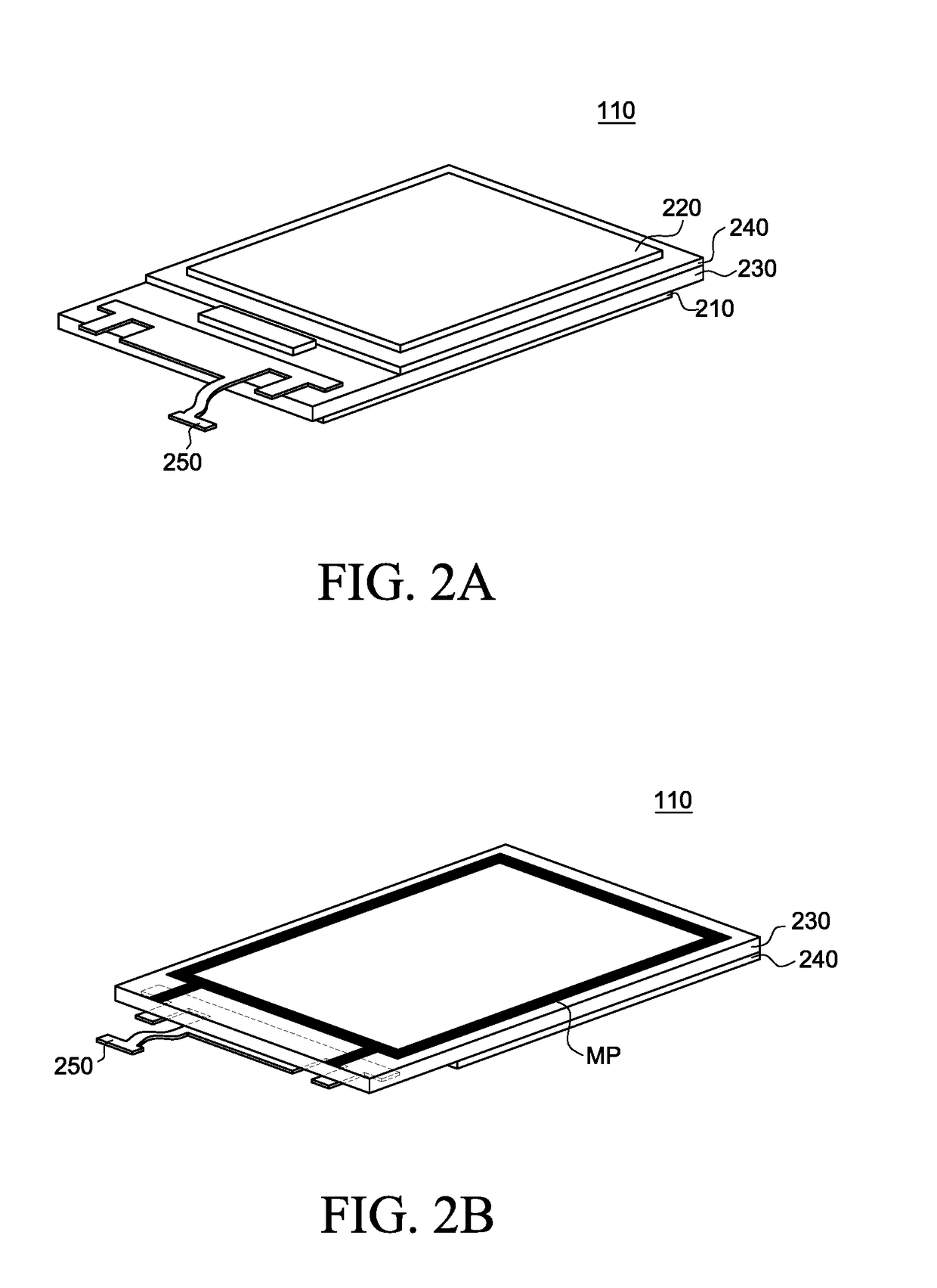
[0018]Still another object to be achieved by an embodiment of the present disclosure is to provide a display device in which a metal pattern is formed continuously along all edges of a bottom surface of a conductive layer, and, thus, an interface between the metal pattern and the conductive layer functions as a path for electrical signals to be applied to the conductive layer and the conductive layer can become an equipotential surface more rapidly.
[0019]Still another object to be achieved by an embodiment of the present disclosure is to provide a display device in which a conductive layer is grounded more stably by a metal pattern, and, thus, a noise of a user's touch signal sensed by an in-cell capacitive touch sensor can be minimized.
[0020]Still another object to be achieved by an embodiment of the present disclosure is to provide a display device in which static electricity accumulated in the display device is effectively discharged through a conductive layer by a metal pattern.

Problems solved by technology

Thus, the interference between the touch sensor and the other components needs to be considered.
However, due to the industry trend toward ultra-slim display panels, unintended interference has not been addressed to satisfaction.
Such a change may deteriorate a touch function.
Such a change may deteriorate an image quality.
Furthermore, since a pressure-sensitive touch sensor and an in-cell capacitive touch sensor are embedded together, interference may occur between the two touch sensors.
Such interference may deteriorate a touch sensing accuracy.

Method used


Image

  • Display device
  • Display device
  • Display device

Examples


Embodiment Construction

[0046]Advantages and features of the present disclosure, and methods for accomplishing the same will be more clearly understood from various exemplary embodiments described below with reference to the accompanying drawings. However, the present disclosure is not limited to the following exemplary embodiments but may be implemented in various different forms. The various exemplary embodiments are provided only to complete disclosure of the present disclosure and to fully provide a person having ordinary skill in the art to which the present disclosure pertains with the category of the disclosure, and the present disclosure will be defined by the appended claims.

[0047]The shapes, sizes, ratios, angles, numbers, and the like shown in the accompanying drawings for describing the exemplary embodiments of the present disclosure are merely examples, and the present disclosure is not limited thereto.

[0048]Throughout the whole specification, the same reference numerals denote the same elemen...


PUM


Abstract

Provided is a display device that includes a display panel defined with an active area displaying an image and an inactive area outside the active area, the display panel including a substrate having a first surface and a second surface opposite the first surface; a plurality of pixels on the first surface of the substrate in the active area, each pixel including a pixel drive circuit; a transparent conductive layer on the second surface of the substrate covering the active area and a part of the inactive area; and a metal pattern on the second surface of the substrate in the inactive area, the metal pattern electrically connected to the transparent conductive layer, receiving an electrical signal and having a lower resistance than the transparent conductive layer, wherein the metal pattern serves as a conductive path to reduce a potential difference with respect to the electrical signal in an entire area of the transparent conductive layer compared to a display device without the metal pattern.

Description

CROSS-REFERENCE TO RELATED APPLICATIONS[0001]This application claims the priority of Korean Patent Application No. 10-2015-0152833 filed on Oct. 31, 2015 and Korean Patent Application No. 10-2015-0190310 filed on Dec. 30, 2015, in the Korean Intellectual Property Office, the disclosure of which is incorporated herein by reference for all purposes as if fully set forth herein.BACKGROUND[0002]Field[0003]The present disclosure relates to a display device and a method of manufacturing the same and more particularly, to a display device including an in-cell touch sensor.[0004]Description of the Related Art[0005]Conventionally, a touch screen panel has been manufactured separately and then bonded to a display panel when implementing a display device capable of recognizing a user's touch. That is, a touch electrode has been formed separately using a glass substrate, a plastic substrate, a film or a sheet as a supporting member. Then, the supporting member on which the touch electrode is fo...

Claims


Application Information

Patent Timeline
Patent Type & Authority Applications(United States)
IPC IPC(8): G06F3/044
CPCG06F2203/04103G06F3/044G06F3/041G06F2203/04107
Inventor JO, HEUNGJUPARK, JEONGKWEONPARK, CHANKWON, SANGHYUN
Owner LG DISPLAY CO LTD
Why Eureka
Try Eureka