Semiconductor device, package, and vehicle

a semiconductor and package technology, applied in the field of semiconductor devices, can solve the problems of increasing the projected area of semiconductor devices, reducing the signal quality of analog circuits, and increasing the mounting area, so as to speed up the semiconductor chip, reduce jitter, and ensure the reliability of semiconductor operation.

Inactive Publication Date: 2017-06-08
PANASONIC INTELLECTUAL PROPERTY MANAGEMENT CO LTD
View PDF5 Cites 6 Cited by
  • Summary
  • Abstract
  • Description
  • Claims
  • Application Information

AI Technical Summary

Benefits of technology

[0021]The present disclosure is intended to solve the above-described problem, and to achieve reliable operation of a semiconductor and reduction of jitters even when signal processing is performed at high speed.
[0022]A semiconductor device according to an aspect of the present disclosure includes a metal plate capacitor including a heat-resistant metal plate and a capacitor unit that is formed on at least one surface of the heat-resistant metal plate, a semiconductor chip disposed on the metal plate capacitor, a connector configured to electrically connect the semiconductor chip and the capacitor, and a protector configured to protect the semiconductor chip, the metal plate capacitor, and the connector. The metal plate capacitor is included in the semiconductor device. A capacitor component necessary for speeding-up of the semiconductor chip can be freely supplied to the semiconductor chip, thereby achieving significant reduction of jitters in signal processing, and improved external noise resistance.
[0023]A package according to another aspect of the present disclosure includes a semiconductor device including: a metal plate capacitor including a heat-resistant metal plate and a capacitor unit that is formed on at least one surface of the heat-resistant metal plate; a semiconductor chip disposed on the metal plate capacitor; a connector configured to electrically connect the semiconductor chip and the capacitor; and a protector configured to protect the semiconductor chip, the metal plate capacitor, and the connector, and a wiring substrate on which the semiconductor device is mounted. The metal plate capacitor is included in the semiconductor device. A capacitor component necessary for speeding-up of the semiconductor chip can be freely supplied to the semiconductor chip, thereby achieving significant reduction of jitters in signal processing, and improved external noise resistance.
[0024]A vehicle according to another aspect of the present disclosure is a vehicle on which a package is mounted, the package including a semiconductor device including: a metal plate capacitor including a heat-resistant metal plate and a capacitor unit that is formed on at least one surface of the heat-resistant metal plate; a semiconductor chip disposed on the metal plate capacitor; a connector configured to electrically connect the semiconductor chip and the capacitor; and a protector configured to protect the semiconductor chip, the metal plate capacitor, and the connector, and a wiring substrate on which the semiconductor device is mounted. The metal plate capacitor is included in the semiconductor device. A capacitor component necessary for speeding-up of the semiconductor chip can be freely supplied to the semiconductor chip, thereby achieving significant reduction of jitters in signal processing, improved external noise resistance, and speeding-up of signal processing in the vehicle.
[0025]According to the present disclosure, a capacitance component necessary for speeding-up of a semiconductor chip can be freely supplied from a metal plate capacitor to the semiconductor chip. This can achieve significant reduction of jitters in signal processing, improved external noise resistance, and noise reduction in high-speed signal processing in, for example, a vehicle.

Problems solved by technology

However, in such a conventional semiconductor device, when high-speed signal processing is performed, jitters cause a problem.
However, when the semiconductor chip and the laminated ceramic capacitor are disposed on an identical surface, an increased mount area is needed, which is a problem.
As a result, the semiconductor device has an increased projected area, which is another problem.
When the jitter value is increased, for example, data error in a digital circuit is caused in some cases, and a signal quality in an analog circuit decreases in some cases.
However, when capacitor unit 11 is formed by using TAB 7, it is difficult to satisfy characteristics required for a bypass capacitor.
In addition, it is difficult to form a ceramic sinter film having a high dielectric constant.
This is partly because it is difficult to perform high temperature processing at 400° C. or higher when the TAB tape is used.
This is because a polyimide material used as the TAB tape is not resistant to a temperature of 400° C. or higher.
As a result, it is often difficult to form a large-capacity bypass capacitor that is not degraded through high speed signal processing, and thus provides an effect of reducing variation of power-supply voltage.
As described above, a conventional heat-resistant metal material cannot be used in place of the TAB to form a capacitor.
These metal materials, which have excellent thermal resistances, have such a problem that, when the materials are fabricated as a lead frame having a fine pattern and subjected to thermal processing at high temperatures of 300° C. or higher, 600° C. or higher, and 900° C. or higher, a fine part is likely to deform.
In other words, when a capacitor is formed on a heat-resistant metal plate shaped in a lead frame having a fine pattern through thermal processing at high temperatures of 300° C. or higher, and 400° C. or higher, a polyimide reinforced portion provided to prevent a dimensional change at a fine part becomes deformed and burnt during heating, resulting in a largely decreased dimensional accuracy of the lead frame.

Method used


Image

  • Semiconductor device, package, and vehicle
  • Semiconductor device, package, and vehicle
  • Semiconductor device, package, and vehicle

Examples


first exemplary embodiment

[0115]The semiconductor device according to the present disclosure and the vehicle including the semiconductor device will be described as the first exemplary embodiment with reference to FIG. 1A and FIG. 1B.

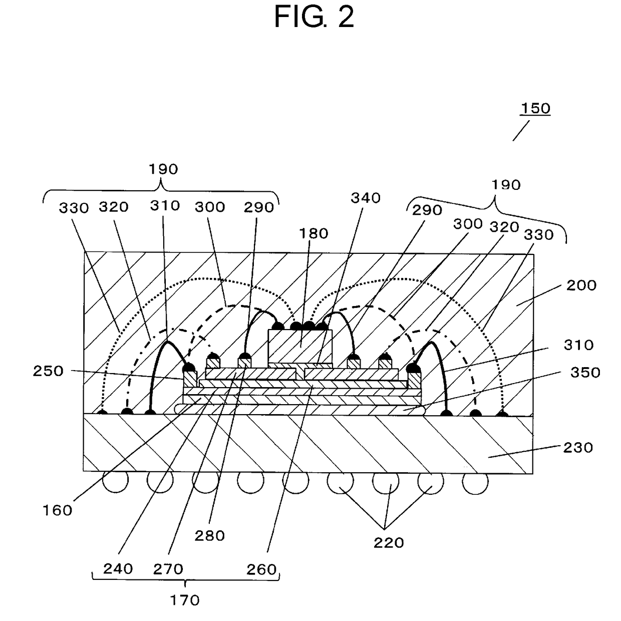
[0116]FIG. 1A is a top view for description of an exemplary vehicle according to the present disclosure, and FIG. 1B is a sectional view illustrating an exemplary semiconductor device according to the present disclosure.

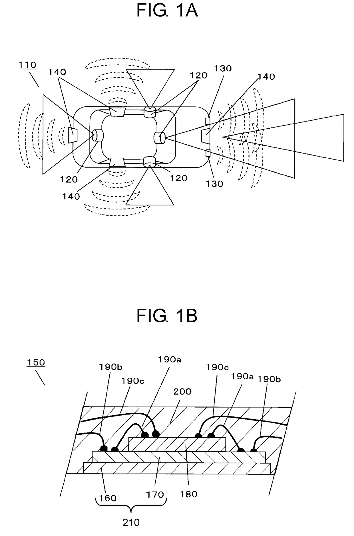
[0117]Vehicle 110 illustrated in FIG. 1A includes the semiconductor device according to the present disclosure. As illustrated in FIG. 1A, it is proposed to incorporate various devices in vehicle 110 to improve travel safety.

[0118]In FIG. 1A, cameras 120 are incorporated in front, side, and rear parts of vehicle 110. Laser radar 130 and milliwave radar 140 are incorporated in the front and side parts of vehicle 110. Improving safety of vehicle 110 when, for example, traveling requires incorporation of various sensors such as cameras 120, laser radar 130, and mill...

second exemplary embodiment

[0245]The second exemplary embodiment describes an example in which a lead frame is used in place of resin substrate unit 230 used in the first exemplary embodiment.

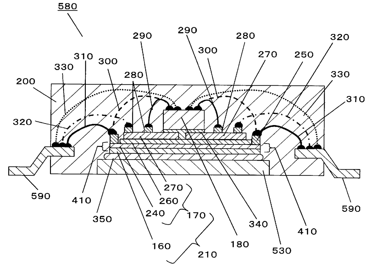
[0246]FIG. 21 is a sectional view for description of an exemplary semiconductor device as an example of the present disclosure when a lead frame is used in place of the resin substrate. In FIG. 21, lead frame 590 is used in place of resin substrate unit 230 illustrated in FIGS. 2 to 17 described above. No significant difference is present except for the above-described point. Description of any matter shared with the first exemplary embodiment will be omitted in some cases. For example, a QFP is known as the semiconductor device illustrated in FIG. 21, but the example of the present disclosure does not need to be limited to the QFP.

[0247]Semiconductor device 580 illustrated in FIG. 21 includes lead frame 590, metal plate capacitor 210 including heat-resistant metal plate 160, and lower electrode 240, sintered dielectric ...

third exemplary embodiment

[0283]The following describes, as a third exemplary embodiment, improvement of connection of semiconductor chip 180 and metal plate capacitor 210 with land electrode 480 of resin substrate unit 230 and lead frame leading end part 690 of lead frame 590 with reference to FIGS. 29A to 32.

[0284]The description with reference to FIGS. 29A to 32 is made on the lead frame (or lead frame leading end part 690), but the present exemplary embodiment is applicable to semiconductor device 150 described with reference to FIG. 2 and the like described above when lead frame leading end part 690 is replaced with land electrode 480 in resin substrate unit 230.

[0285]FIGS. 29A to 29C are each a top view or a side view for description of one structure of the metal plate capacitor for optimizing a Vdd line, a Vss line, a signal line, and the like in the semiconductor chip, the metal plate capacitor, and the like.

[0286]In FIG. 29A, semiconductor chip 180 and upper auxiliary electrode 280a are connected wi...


PUM


Abstract

A semiconductor device includes a metal plate capacitor that includes a heat-resistant metal plate and a capacitor unit including a sintered dielectric formed on at least one surface of the heat-resistant metal plate, a semiconductor chip disposed on the metal plate capacitor, a connector configured to electrically connect the semiconductor chip and the metal plate capacitor, and a protector configured to protect the semiconductor chip, the metal plate capacitor, and the connector.

Description

BACKGROUND[0001]1. Technical Field[0002]The present disclosure relates to a semiconductor device included in, for example, an image processing apparatus to achieve improved safety of a vehicle and the like, a package, and a vehicle, and a vehicle and various electronic devices can provide improved performance when the semiconductor device and the package are mounted.[0003]2. Description of the Related Art[0004]Recently, increasing safety has been required for a vehicle. The safety and performance of a vehicle are improved by cameras (optical devices using, for example, visible light and infrared) attached to front and rear sides of the vehicle, and radars (using, for example, ultrasonic, laser, and milliwaves). In addition, for example, a HDMI (registered trademark) device is used in the field of in-vehicle communication with devices mounted on a vehicle, and the field of high speed communication with portable terminals.[0005]A semiconductor device and a package according to the pre...

Claims


Application Information

Patent Timeline
Patent Type & Authority Applications(United States)
IPC IPC(8): H01L23/495H01L23/00B60R11/04H01L23/64H01L23/31H04N5/225H01L49/02H01L23/498
CPCH01L23/49589B60R2300/301H01L24/48H01L24/16H01L23/49838H01L23/642H01L23/49541H01L23/49568H01L23/3114H04N5/2252B60R11/04H01L2924/1205H01L2224/48265H01L2224/16265B60R2300/105H01L28/65H01L25/00H01L2924/181H01L2224/48091H01L2224/48137H01L2224/48463H01L2224/48464H01L2224/49175H01L2224/73265H01L2224/83101H01L2224/83385H01L2224/92247H01L2924/15192H01L2924/15311H01L2924/19105H01L2924/19107H01L2224/32145H01L2224/48145H01L2224/49113H01L23/367H01L23/49548H01L23/49822H01L23/49861H01L24/49H01L2224/45144H01L2224/45147H01L2224/49433H01L2924/00014H04N23/57H04N23/45H01L2924/00012H01L2924/00H01L2224/05599H04N23/51H01L23/481
Inventor KATSUMURA, HIDENORITOKUNAGA, SHINYASUMITA, MASAYAYOSHIDA, HIROYOSHISUGAYA, YASUHIROURIU, KAZUHIDESHIBATA, OSAMU
Owner PANASONIC INTELLECTUAL PROPERTY MANAGEMENT CO LTD
Why Eureka
Try Eureka