
Transistor substrate and display device

Active Publication Date: 2017-06-08
JAPAN DISPLAY INC
View PDF2 Cites 5 Cited by
  • Summary
  • Abstract
  • Description
  • Claims
  • Application Information

AI Technical Summary

Benefits of technology

The invention aims to improve the speed at which signals are processed in a transistor substrate and display device. It reduces the time it takes for a signal to reach the main control circuit, making it faster and more efficient.

Problems solved by technology

Accordingly, there is a risk that the touch detection property or the display property of the display device deteriorates as the sum of the resistance in the ON-state of the switching unit and the resistance of the portion of the power supply wire between the corresponding switching unit and the control circuit increases in the drive electrode which is far from the control circuit.

Method used


Image

  • Transistor substrate and display device
  • Transistor substrate and display device
  • Transistor substrate and display device

Examples


embodiment

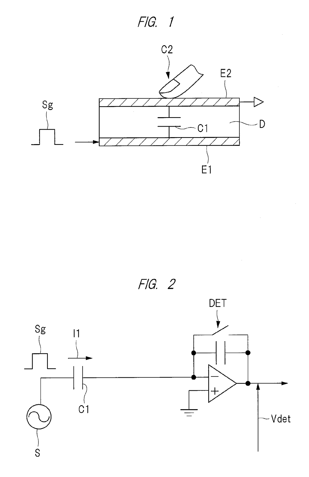
[0044]Hereinafter, a description will be given regarding an example in which a display device is applied to a touch detection function-equipped liquid crystal display device as an embodiment. Herein, the touch detection function-equipped liquid crystal display device is a liquid crystal display device in which a detection electrode for touch detection is provided in any one of an array substrate and a counter substrate included in the display device. In addition, a description will be further given in the embodiment regarding an in-cell type touch detection function-equipped liquid crystal display device having a characteristic that a drive electrode is provided to operate as a drive electrode of a touch panel.

[0045]First, a description will be given regarding a principle of touch detection in a display device according to this embodiment with reference to FIGS. 1 and 2. FIG. 1 is an explanatory diagram illustrating a state in which a finger is in contact or proximity with a touch d...


PUM


Abstract

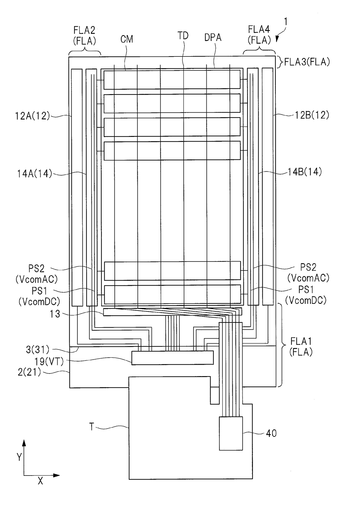
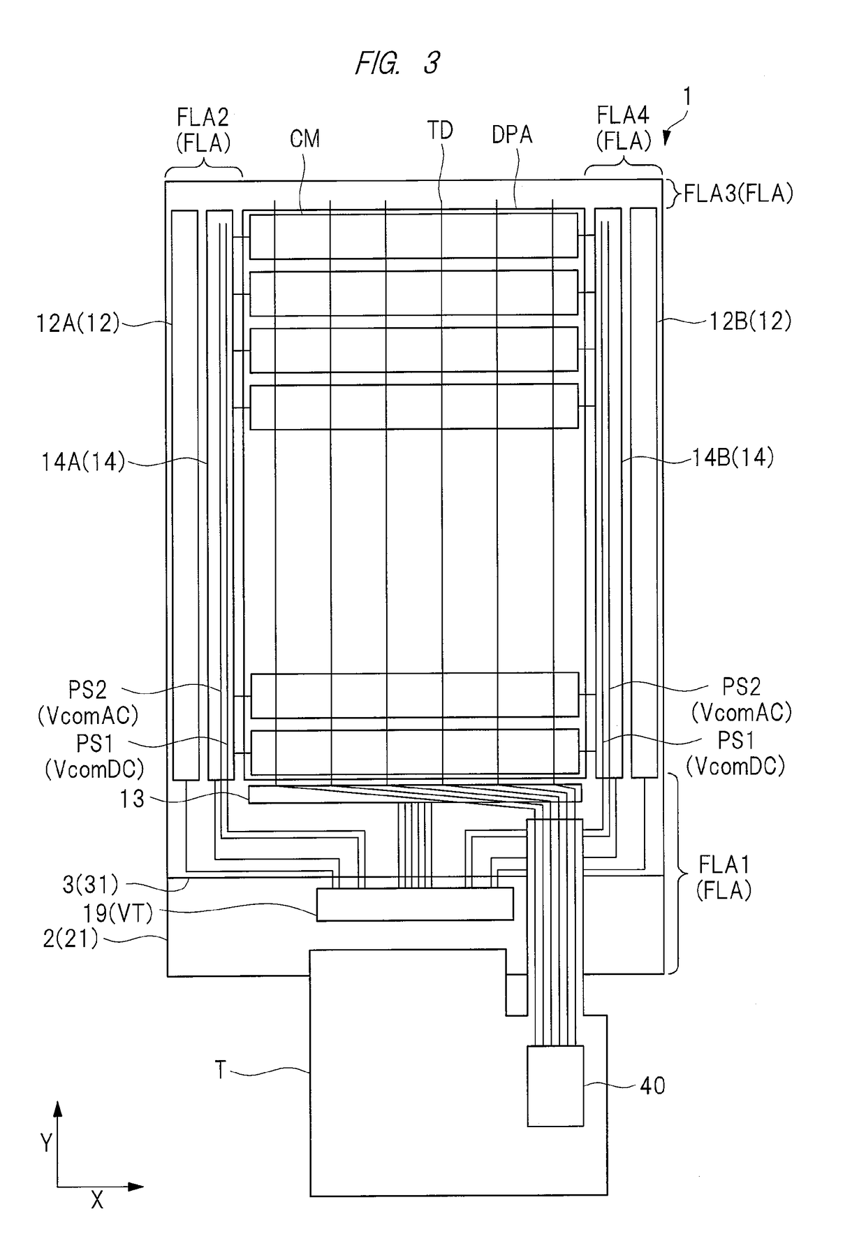
A transistor substrate includes a plurality of first transistors formed between a power supply wire and a first conductive wire, and a plurality of second transistors formed between the power supply wire and a second conductive wire. A length of a portion of the power supply wire between the plurality of second transistors and a drive signal generation circuit is longer than a length of a portion of the power supply wire between the plurality of first transistors and the drive signal generation circuit, and a total sum of channel widths of second channels included in the plurality of second transistors is wider than a total sum of channel widths of first channels included in the plurality of first transistors.

Description

CROSS-REFERENCE TO RELATED APPLICATION[0001]The present application claims priority from Japanese Patent Application No. 2015-235989 filed on Dec. 2, 2015, the content of which is hereby incorporated by reference into this application.TECHNICAL FIELD OF THE INVENTION[0002]The present invention relates to a transistor substrate and a display device and for example, relates to a technique which is effectively applied to a transistor substrate including a plurality of transistors and a display device.BACKGROUND OF THE INVENTION[0003]There are display devices in which a scan signal is supplied to a plurality of pixels provided in a display region through a plurality of scan lines, and a pixel signal is supplied through a plurality of signal lines, thereby displaying an image. In such display devices, there is a demand for reduction in width of a frame region outside the display region in order to reduce a size of the display device and increase the display region.[0004]The plurality of ...

Claims


Application Information

Patent Timeline
IPC IPC(8): H01L27/12G02F1/1343G02F1/1362G02F1/1368
CPCH01L27/124G02F2203/04G02F1/13439G02F1/134336G02F1/136286G06F3/0412G02F1/13338G06F3/044G06F2203/04108G09G3/3677G09G3/3688G09G2300/0452G02F1/133514G02F1/133345G02F2201/121G02F2201/123G02F2001/134345G02F1/1368G02F1/133G02F1/1362H01L27/12H01L27/1214G02F1/13624G06F3/04164G06F3/0445G06F3/0446H01L27/1255G02F1/134345
Inventor KOIDE, GEN
Owner JAPAN DISPLAY INC
Learn More