Camera Module and Optical Apparatus

a technology of optical apparatus and camera module, which is applied in the direction of television system, printed circuit non-printed electric components association, instruments, etc., to achieve the effect of reducing the distance between the upper surface of the image sensor and the bottom surface of the lens module, reducing the thickness of the base, and reducing the position of the bottom end surfa

Active Publication Date: 2017-07-27
LG INNOTEK CO LTD
View PDF5 Cites 12 Cited by
  • Summary
  • Abstract
  • Description
  • Claims
  • Application Information

AI Technical Summary

Benefits of technology

[0066]An FBL (Flange Back Length), a distance from an upper surface of an image sensor to a bottom surface of a lens module can be minimized, through the first exemplary embodiment of the present disclosure.
[0067]A thickness of a base can be reduced by opening a ceiling of a base at an upper side of a circuit element, through the modification according to the first exemplary embodiment of the present disclosure.
[0068]Furthermore, it may be possible to reduce a position of a bottom end surface of a lens driving unit when a relevant design is applied.
[0069]An IR (Infrared) introduction space can be enlarged by securing a space between a corner of a sensor base and a corner of a lens driving unit, through the second exemplary embodiment of the present disclosure.
[0070]Furthermore, it is possible to increase a temporary stability for a lens position due to obtainment of IR curing energy.
[0071]Still furthermore, productivity can be increased by decrease in a curing time.

Problems solved by technology

However, the conventional camera modules having the handshake correction function suffer from disadvantages in that a camera module part alone on the mobile terminal protrudes from the mobile terminal due to increased whole length of the camera module, which is resultant from use of the handshake correction function.
On the other hand, the conventional camera module suffers from drawbacks in that the temporary curing for assembly of a camera module is not performed in a proper manner to twist a position during movement; and a time for temporary curing process becomes increased in order to integrate temporary adhesion stability.

Method used


Image

  • Camera Module and Optical Apparatus
  • Camera Module and Optical Apparatus
  • Camera Module and Optical Apparatus

Examples


Embodiment Construction

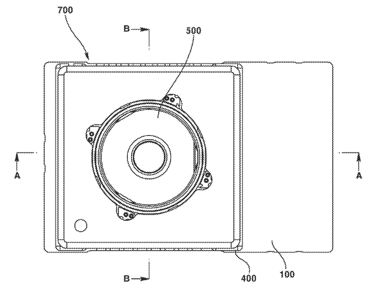
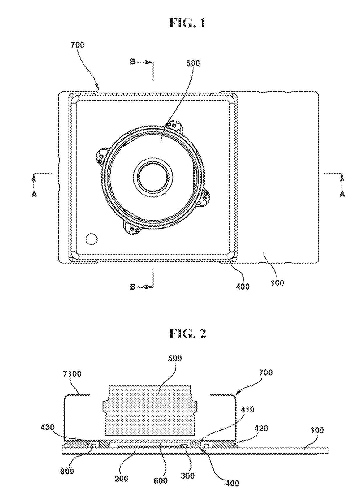
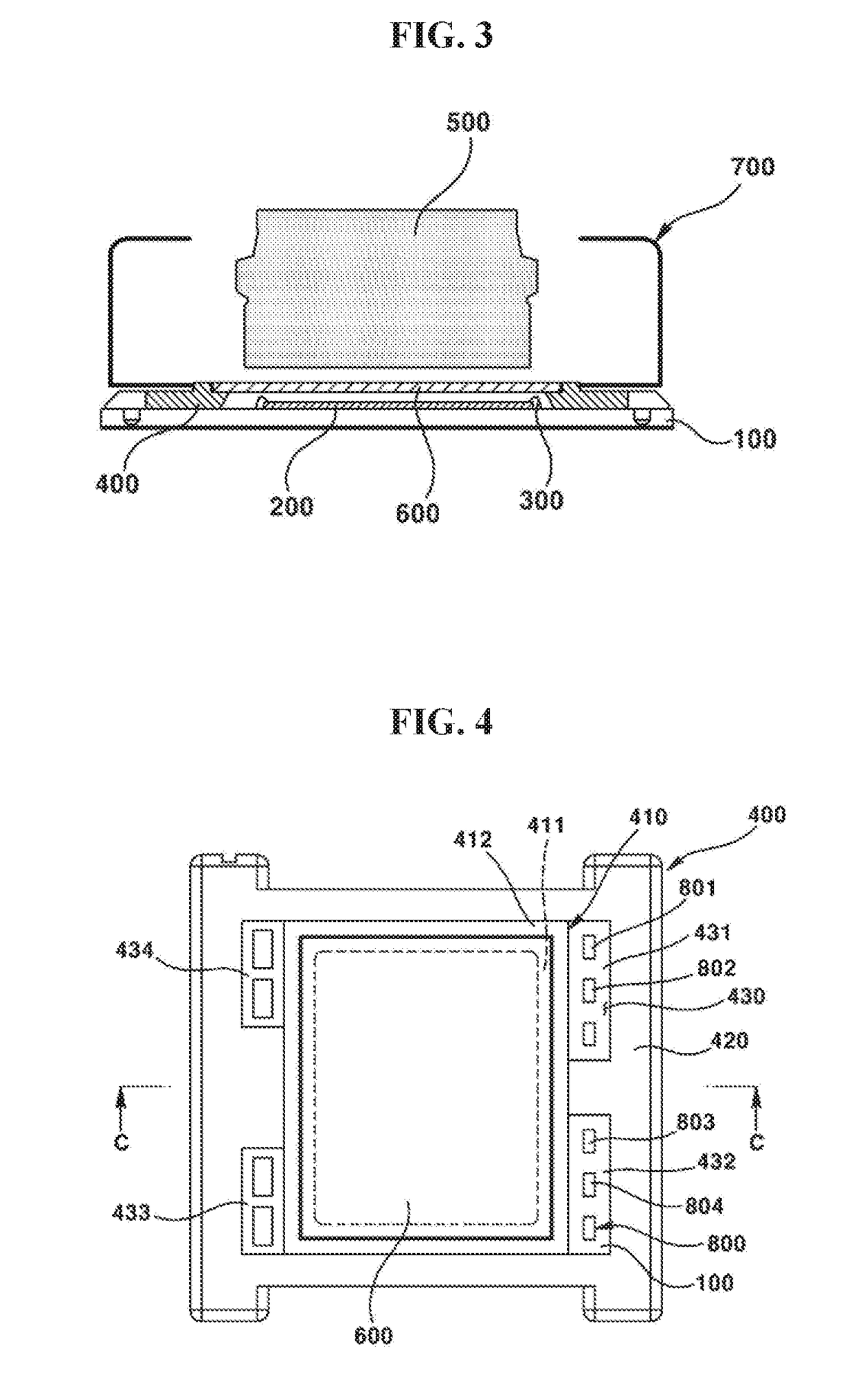
[0086]Hereinafter, exemplary embodiments of the present disclosure are described in detail with reference to the accompanying drawings. It will be appreciated that for simplicity and / or clarity of illustration, elements illustrated in the figure have not necessarily been drawn to scale. For example, the dimensions of some of the elements may be exaggerated relative to other elements for clarity. Accordingly, in some embodiments, well-known processes, well-known device structures and well-known techniques are not illustrated in detail to avoid unclear interpretation of the present disclosure. The same reference numbers will be used throughout the specification to refer to the same or like parts.

[0087]It will be understood that, although the terms first, second, A, B, (a), (b), etc. may be used herein to describe various elements, components, regions, layers, and / or sections, these elements, components, regions, layers, and / or sections should not be limited by these terms. These terms...


PUM


Abstract

The present disclosure relates to a camera module, the camera module including a circuit board, an image sensor disposed on an upper surface of the circuit board, a current carrying part electrically connecting the image sensor and the circuit board, and a base disposed on the upper surface of the circuit board, wherein the base is not overlapped with the image sensor and the current carrying part in a direction of an optical axis.

Description

CROSS-REFERENCE TO RELATED APPLICATIONS[0001]This application claims priority under 35 U.S.C. §119 to Korean Patent Application Nos. 10-2016-0008532 and 10-2016-0008534, filed Jan. 25, 2016; and 10-2016-0010739, filed Jan. 28, 2016, which are hereby incorporated by reference in their entirety.TECHNICAL FIELD[0002]Exemplary embodiments of the present disclosure may relate to a camera module and an optical apparatus.BACKGROUND[0003]The technology described in this section is merely intended to provide background, information of an exemplary embodiment of the present disclosure, and does not mean the prior art.[0004]Concomitant with wide propagation of various mobile terminals (smart phones) and commercialization of wireless Internet services, demands by consumers related to the mobile terminals are diversified, and various types of additional equipment are attached to the mobile terminals.[0005]Among the various types of additional equipment, a camera module may be a representative de...

Claims


Application Information

Patent Timeline
Patent Type & Authority Applications(United States)
IPC IPC(8): H04N5/225G02B7/09H05K1/18G02B27/64
CPCH04N5/2257H04N5/2253H04N5/2254G02B27/646H04B1/3827H05K1/181H05K2201/10121H05K2201/10151H04M1/0264G02B7/09G02B7/08H04N23/54H04N23/57H04N23/55
Inventor HA, TAE MINOH, HYUN AH
Owner LG INNOTEK CO LTD
Why Eureka
Try Eureka