Array substrate and method of manufacturing the same, display panel and display device

a display panel and substrate technology, applied in semiconductor devices, instruments, optics, etc., can solve the problems of narrow viewing angle, low contrast and color distortion, and low viewing angle of existing display devices, and achieve the effect of improving the viewing angle of a display devi

Active Publication Date: 2017-08-03
BOE TECH GRP CO LTD
View PDF1 Cites 7 Cited by
  • Summary
  • Abstract
  • Description
  • Claims
  • Application Information

AI Technical Summary

Benefits of technology

[0007]An object of the present disclosure is to provide an array substrate, for improving the viewing angle of a display device.
[0010]In the array substrate provided according to the present disclosure, the voltage compensation unit configured to charge a sub-pixel electrode and the voltage division unit configured to reduce a voltage on a sub-pixel electrode are provided for the sub-pixel electrodes of the pixel unit, and are adjusted such that voltages of respective sub-pixel electrodes are not all the same, thereby deflection angles of liquid crystal molecules located within regions corresponding to the sub-pixel electrode are different from each other, thereby enabling wide viewing-angle display of the display device.
[0011]Another object of the present disclosure is to provide a display panel, for improving the viewing angle of a display device. The display panel comprises the array substrate provided in the above technique scheme. Advantages of the display panel are the same as those of the above array substrate over prior arts and will not be repeatedly described herein.

Problems solved by technology

In a conventional liquid crystal display, liquid crystal molecules are generally driven to deflect by a vertical electric field between a pixel electrode and a common electrode line, thus when viewing from a side of the liquid crystal display, there are low contrast and color distortion, that is, there is a problem related to a narrow viewing angle.
However, since the charges on both two sub-pixel electrodes will be consumed, a voltage difference between the two sub-pixel electrodes may decrease when the charges on the two sub-pixel electrodes are consumed by different amounts, so that a difference between deflection angles of the liquid crystal molecules located within regions corresponding to the two sub-pixel electrodes will be smaller, thereby the improvement of the viewing angle of the liquid crystal display is not significant; in other words, there is still a problem of narrower viewing angle in existing display devices.

Method used


Image

  • Array substrate and method of manufacturing the same, display panel and display device
  • Array substrate and method of manufacturing the same, display panel and display device
  • Array substrate and method of manufacturing the same, display panel and display device

Examples


Embodiment Construction

[0035]In the following, an array substrate, a display panel and a display device according to embodiments of the present disclosure will be further described in detail with reference to the drawings.

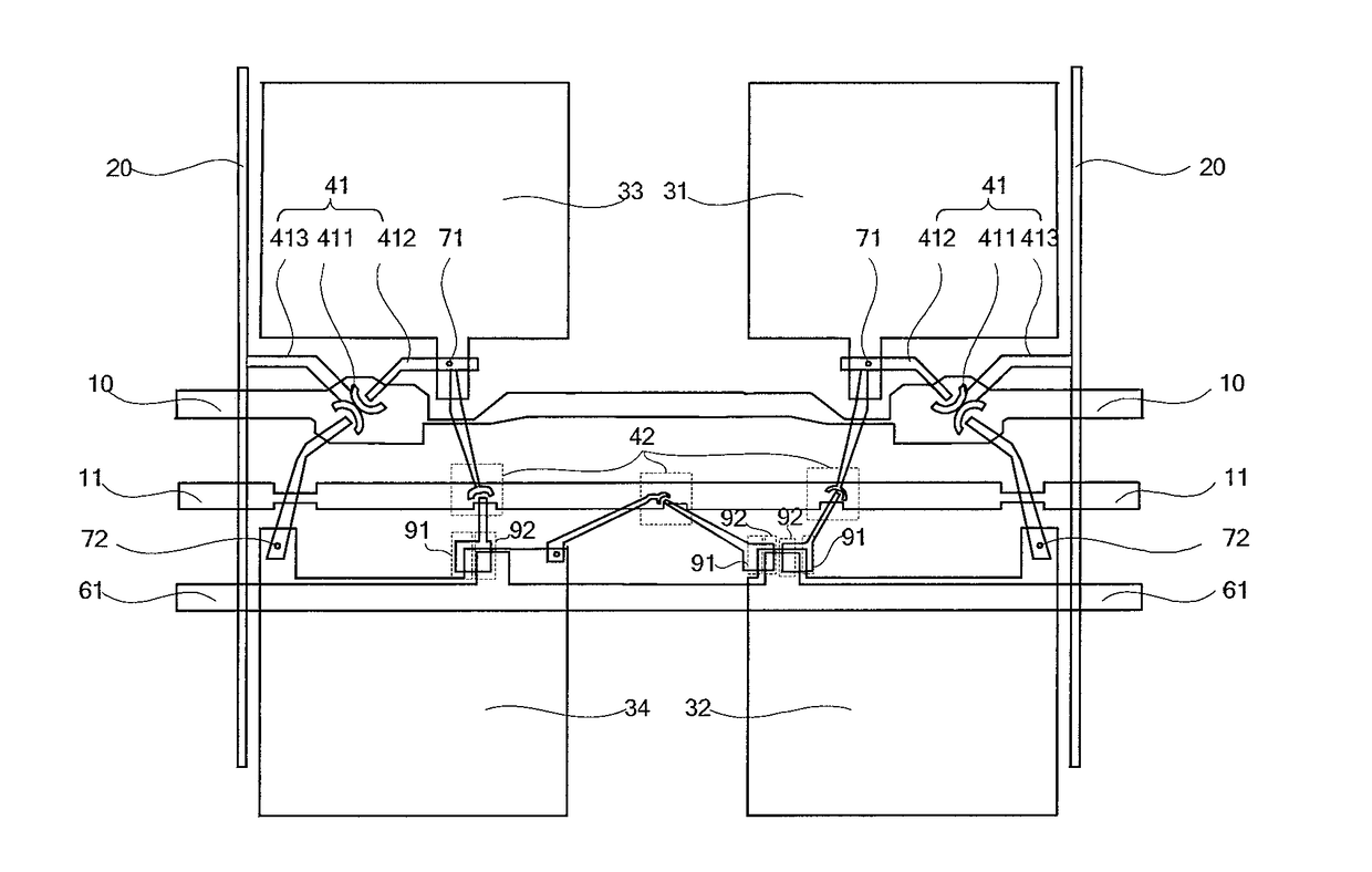
[0036]Referring to FIG. 1, an embodiment of the present disclosure provides an array substrate, comprising a plurality of data lines 20 and a plurality of gate lines 10 arranged to cross each other, and a column of pixel unit being disposed between adjacent data lines 20, each of at least one pixel unit comprises at least two sub-pixel electrodes independent of each other, and first thin film transistors configured to control charging and discharging of corresponding sub-pixel electrodes, for example, a first thin film transistor 41 comprising a gate 411, a drain electrode 412, and a source electrode 413; each of the at least one pixel unit further comprises a voltage compensation unit 51 configured to charge at least one sub-pixel electrode of the pixel unit and a voltage division unit ...


PUM

PropertyMeasurementUnit
voltageaaaaaaaaaa
widthaaaaaaaaaa
lengthaaaaaaaaaa

Abstract

The disclosure provides an array substrate, a display panel and a display device, for increasing a viewing angle of the display device. The array substrate includes a plurality of data lines and a plurality of gate lines arranged to cross each other, and a column of pixel units between adjacent data lines, at least one pixel unit each includes at least two sub-pixel electrodes, a voltage compensation unit for charging at least one sub-pixel electrode of the pixel unit and a voltage division unit for reducing a voltage on at least one of other sub-pixel electrodes of the pixel unit. The voltage compensation unit and the voltage division unit are adjusted such that voltages on sub-pixel electrodes are not all the same, thereby deflection angles of liquid crystal molecules located within regions corresponding to the sub-pixel electrode are different from each other, enabling wide viewing-angle display of the display device.

Description

BACKGROUND[0001]Technical Field[0002]Embodiments of the present disclosure generally relate to the field of display technologies, and particularly, to an array substrate, a display panel and a display device.[0003]Description of the Related Art[0004]Liquid crystal display has become dominant in flat panel display recently due to its characteristics such as small volume, low power consumption, no radiation and the like. The size of the liquid crystal display has become larger and larger, thus there is higher requirement for a range of viewing angle of the liquid crystal display.[0005]In a conventional liquid crystal display, liquid crystal molecules are generally driven to deflect by a vertical electric field between a pixel electrode and a common electrode line, thus when viewing from a side of the liquid crystal display, there are low contrast and color distortion, that is, there is a problem related to a narrow viewing angle. In order to solve the above problem, there has proposed...

Claims


Application Information

Patent Timeline
Patent Type & Authority Applications(United States)
IPC IPC(8): G02F1/1343H01L27/12G02F1/1368G02F1/1333G02F1/1362
CPCG02F1/134309G02F1/133345G02F1/136286G02F1/1368G02F1/13439G02F2201/121H01L27/1255H01L27/1259G02F2001/134345G02F2201/123H01L27/124G02F1/136213G02F1/13624G02F1/134345
Inventor LI, WENBOCHENG, HONGFEILI, PANXIAN, JIANBO
Owner BOE TECH GRP CO LTD
Why Eureka
Try Eureka