

Access control method, bus system, and semiconductor device
- Summary
- Abstract
- Description
- Claims
- Application Information
AI Technical Summary
Benefits of technology
Problems solved by technology
Method used
Image

Examples
operation example 1
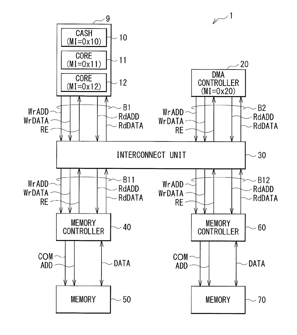
[0077]First, an operation example 1 is described in which the cash 10 of the information processing unit 9 makes the write request by the posted transfer to the memory 50.
[0078]FIG. 6 illustrates the operation example 1 of the bus system 1. In FIG. 6, a signal denoted by a thick solid line denotes a signal that becomes active prior to the timing of the generation of the response signal RE. A signal denoted by a thick broken line denotes a signal that becomes active after the timing of the generation of the response signal RE.
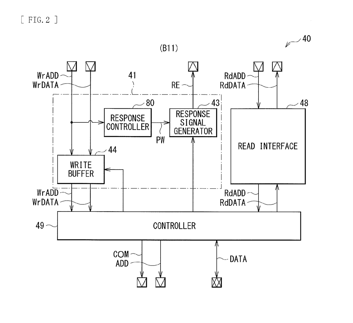
[0079]First, the cash 10 of the information processing unit 9 may make the write request by the posted transfer to the memory 50. In one specific example, the information processing unit 9 may generate the write address WrADD and the write data WrDATA. The information processing unit 9 may supply the write address WrADD and the write data WrDATA to the interconnect unit 30. The write address WrADD may include the identifier MI of the cash 10 (“0x10”) and the tra...
operation example 2
[0083]Next, an operation example 2 is described in which the DMA controller 20 makes the write request by the posted transfer to the memory 50.
[0084]FIG. 7 illustrates the operation example 2 of the bus system 1. First, the DMA controller 20 may make the write request by the posted transfer to the memory 50. In one specific example, the DMA controller 20 may generate the write address WrADD and the write data WrDATA. The DMA controller 20 may supply the write address WrADD and the write data WrDATA to the interconnect unit 30. The write address WrADD may include the identifier MI of the DMA controller 20 (“0x20”) and the transfer mode information MODE having the value of “1” (MODE=1). The memory controller 40 may receive the write address WrADD and the write data WrDATA, through the interconnect unit 30. Moreover, the memory controller 40 may allow the write buffer 44 to temporarily store the write address WrADD and the write data WrDATA.
[0085]The response controller 80 of the memor...
operation example 3
[0088]Next, an operation example 3 is described in which the cash 10 of the information processing unit 9 makes the write request by the posted transfer to the memory 70.
[0089]FIG. 8 illustrates the operation example 3 of the bus system 1. First, the cash 10 of the information processing unit 9 may make the write request by the posted transfer to the memory 70. In one specific example, the information processing unit 9 may generate the write address WrADD and the write data WrDATA. The information processing unit 9 may supply the write address WrADD and the write data WrDATA to the interconnect unit 30. The write address WrADD may include the identifier MI of the cash 10 (“0x10”) and the transfer mode information MODE having the value of “1” (MODE=1). The memory controller 60 may receive the write address WrADD and the write data WrDATA, through the interconnect unit 30. Moreover, the memory controller 60 may allow the write buffer 64 to temporarily store the write address WrADD and...
PUM
 Abstract
Description
Claims
Application Information