Conductive device substrate, method for manufacturing conductive device substrate, and display panel

a technology of conductive devices and substrates, applied in semiconductor devices, instruments, electrical devices, etc., can solve the problems of difficulty in mass production and low yield, and achieve the effect of effectively reducing border space and maintaining yield

Inactive Publication Date: 2017-09-07
AU OPTRONICS CORP
View PDF8 Cites 3 Cited by
  • Summary
  • Abstract
  • Description
  • Claims
  • Application Information

AI Technical Summary

Benefits of technology

[0007]The present disclosure provides a conductive device substrate, a method for manufacturing the conductive device substrate, and a display panel, which can effectively reduce the border space while maintaining the yield.

Problems solved by technology

However, in the existing mature manufacturing process technologies of display, the manufacturing process of drilling a hole on the substrate and filling the hole with the conductive material is complex, resulting in problems such as a low yield and difficulty in realizing mass production.

Method used


Image

  • Conductive device substrate, method for manufacturing conductive device substrate, and display panel
  • Conductive device substrate, method for manufacturing conductive device substrate, and display panel
  • Conductive device substrate, method for manufacturing conductive device substrate, and display panel

Examples


Embodiment Construction

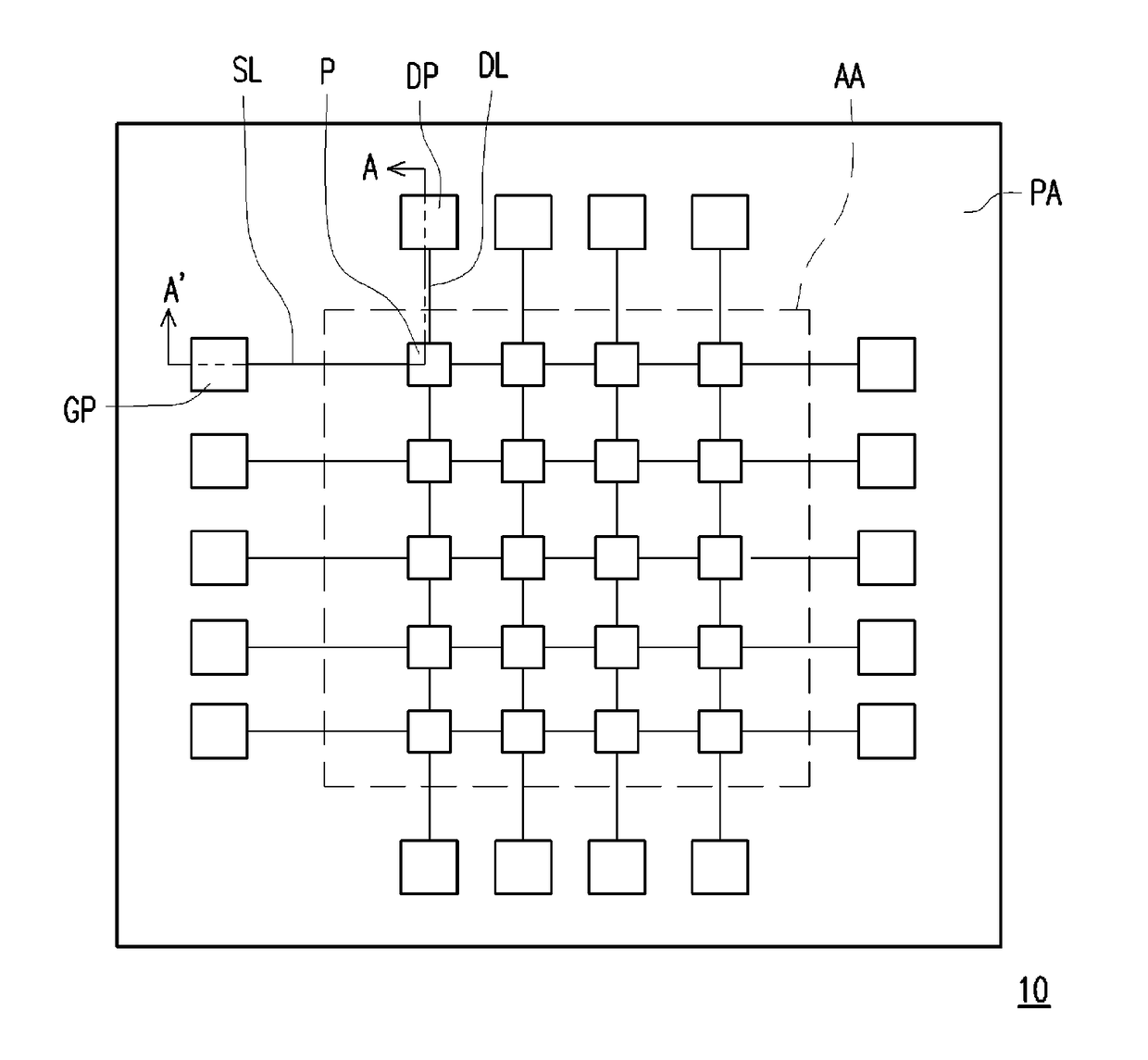
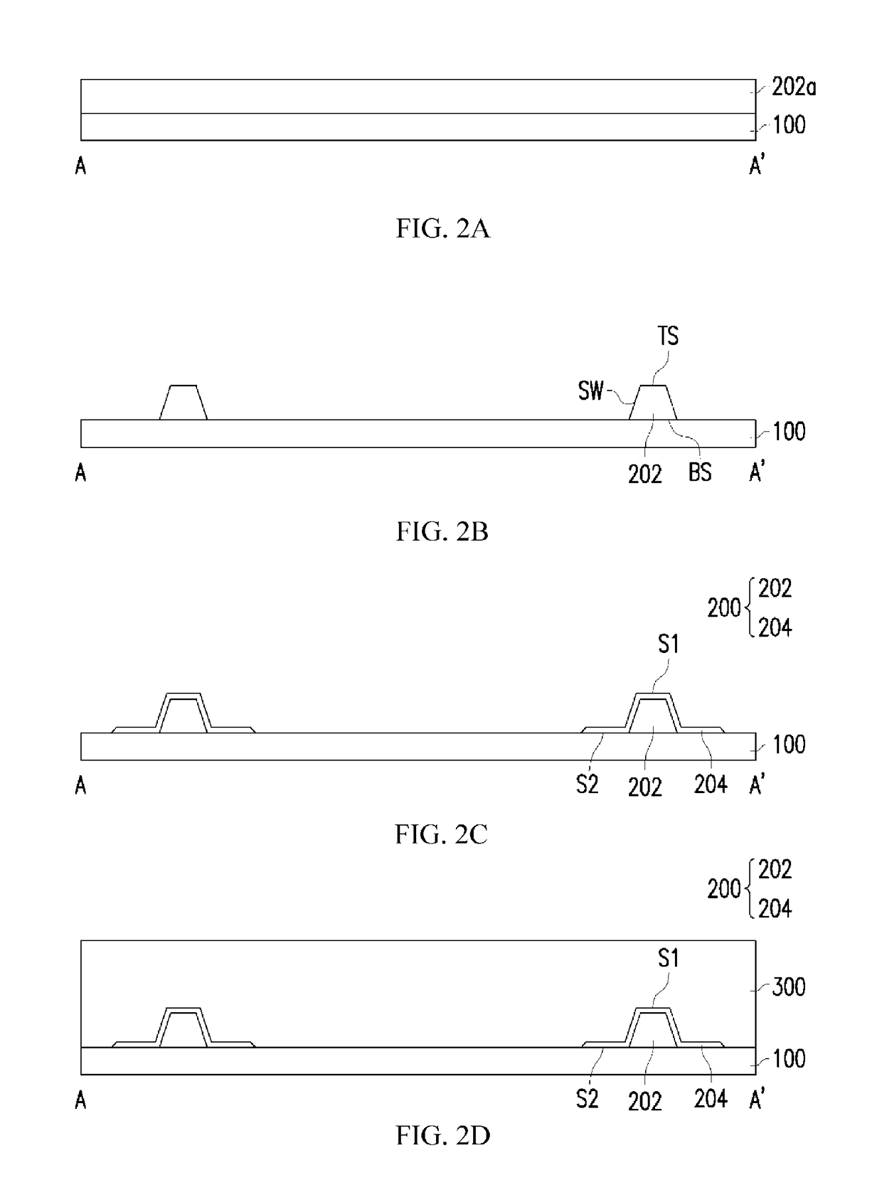
[0020]The following describes the embodiments with reference to the accompanying drawings in detail, so as to make the aspects of present disclosure more comprehensible. However, the mentioned embodiments are not intended to limit the scope of present disclosure, and the description of the operation of a structure is not intended to limit an execution sequence. Any device with equivalent functions that is produced from a structure formed by a recombination of elements shall fall within the scope of present disclosure. Besides, according to industry standards and practices, the drawings are merely intended to assist the description, and are not drawn according to original dimensions. In practice, dimensions of various features may be arbitrarily increased or decreased to facilitate the description. Same elements in the description below are indicated by a same reference sign, so as to facilitate the comprehension.

[0021]In present disclosure, when an element is “connected” or “coupled...


PUM


Abstract

The disclosure provides a method for manufacturing a conductive device substrate. First, a carrier substrate is provided and an organic pillar is formed on the carrier substrate. Subsequently, a conductive layer is formed. The conductive layer covers the organic pillar to form a conductive pillar. The conductive pillar has a first surface and a second surface opposite to each other. Next, a substrate material layer is formed to cover the conductive pillar and the carrier substrate, and the substrate material layer includes an organic material. The substrate material layer exposes the first surface of the conductive pillar. Subsequently, a device layer is formed on the substrate material layer to electrically connect to the conductive pillar. In addition, a conductive device substrate and a display panel are also provided.

Description

CROSS-REFERENCE TO RELATED PATENT APPLICATION[0001]This application claims the benefit of priority to Taiwan Patent Application No. 105106465, filed Mar. 3, 2016. The entire content of the above identified application is incorporated herein by reference.[0002]Some references, which may include patents, patent applications and various publications, are cited and discussed in the description of this disclosure. The citation and / or discussion of such references is provided merely to clarify the description of the present disclosure and is not an admission that any such reference is “prior art” to the disclosure described herein. All references cited and discussed in this specification are incorporated herein by reference in their entireties and to the same extent as if each reference was individually incorporated by reference.FIELD[0003]The present invention relates to a conductive device substrate, and in particular, to a conductive device substrate having an organic pillar.BACKGROUND...

Claims


Application Information

Patent Timeline
Patent Type & Authority Applications(United States)
IPC IPC(8): H01L51/52H01L27/32H01L21/77
CPCH01L27/3244H01L51/5246H01L27/124H01L27/1259H01L27/1266G02F1/133305G02F2201/42G02F2202/02G02F1/133302H10K59/131H10K71/80H10K50/8426H10K59/12
Inventor CHEN, CHIA-WEIHUANG, YU-SHENG
Owner AU OPTRONICS CORP
Why Eureka
Try Eureka