Transistor structure with varied gate cross-sectional area

a transistor and cross-sectional area technology, applied in the field of transistors with varied gate cross-sectional areas, can solve the problems of limiting the size of particular structures, affecting the performance of the transistor, and presenting conflicting demands for high-performance fets and high-yield processes in particular, so as to reduce the cross-sectional area of the gate area

Active Publication Date: 2017-09-21
GLOBALFOUNDRIES US INC
View PDF0 Cites 0 Cited by
  • Summary
  • Abstract
  • Description
  • Claims
  • Application Information

AI Technical Summary

Benefits of technology

[0004]A first embodiment of the present disclosure provides a method including: forming a structure including: a semiconductor fin positioned on a substrate, wherein the semiconductor fin includes: a gate area, and a terminal area laterally distal to the gate area, a sacrificial gate positioned on the gate area of the semiconductor fin, and an insulator positioned on the terminal area of the semiconductor fin; removing the sacrificial gate to expose the gate area of the semiconductor fin; reducing a cross-sectional area of the gate area of the semiconductor fin; and forming a transistor gate on the gate area of the semiconductor fin.

Problems solved by technology

Over time, improvements to the structure and performance of a transistor, in addition to the ever-decreasing size of these components, have presented significant technical and manufacturing challenges.
FinFETs in particular present conflicting demands for high yield processes and high-performance FETs.
In some cases, the need to couple one component to another may limit the size of particular structures even when a remainder of the same structure can be reduced in size.
As a result, the ability to fully realize spatial improvements to some circuit elements may be limited by competing physical constraints on an IC product.

Method used


Image

  • Transistor structure with varied gate cross-sectional area
  • Transistor structure with varied gate cross-sectional area
  • Transistor structure with varied gate cross-sectional area

Examples


Embodiment Construction

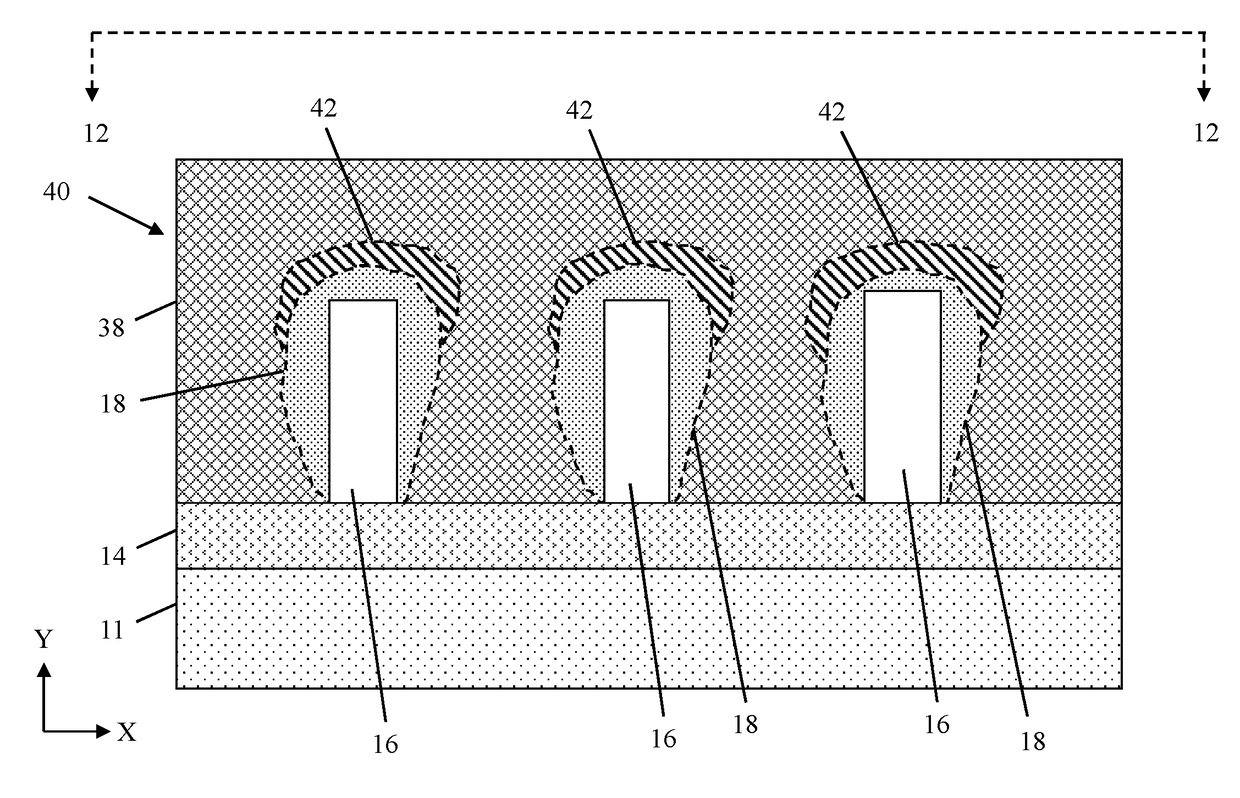
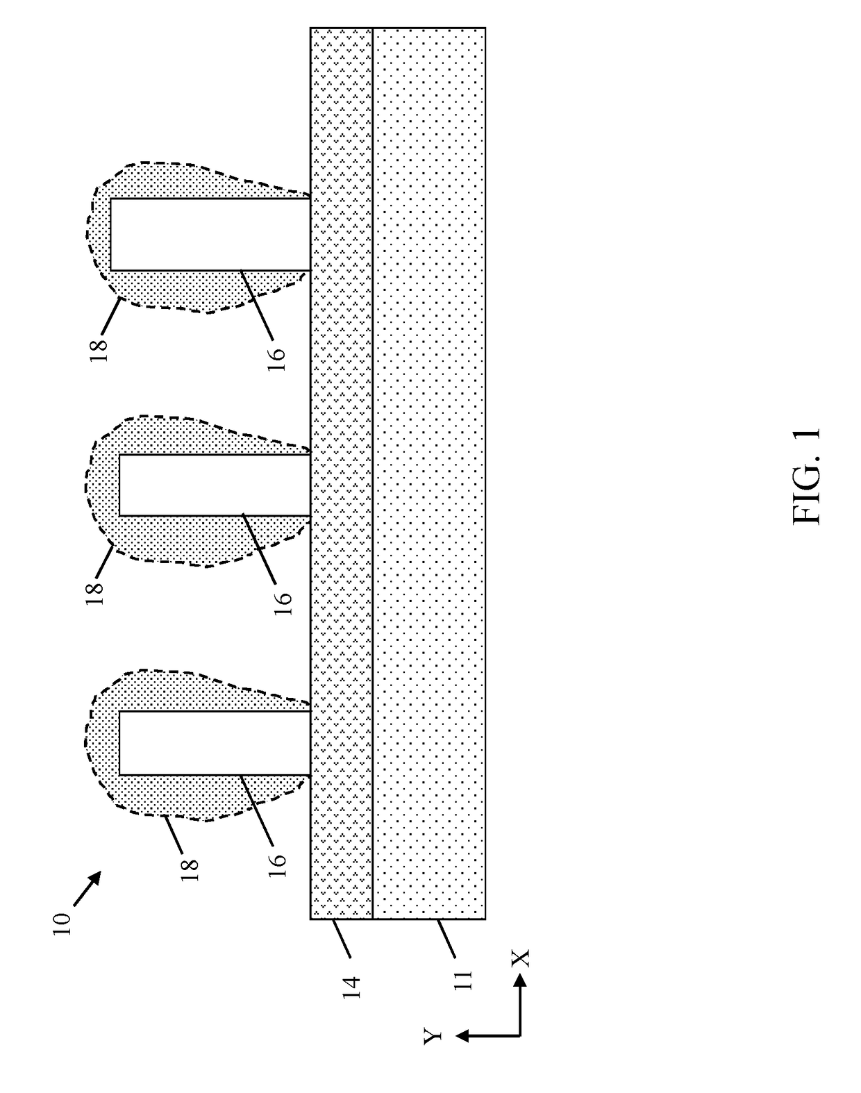
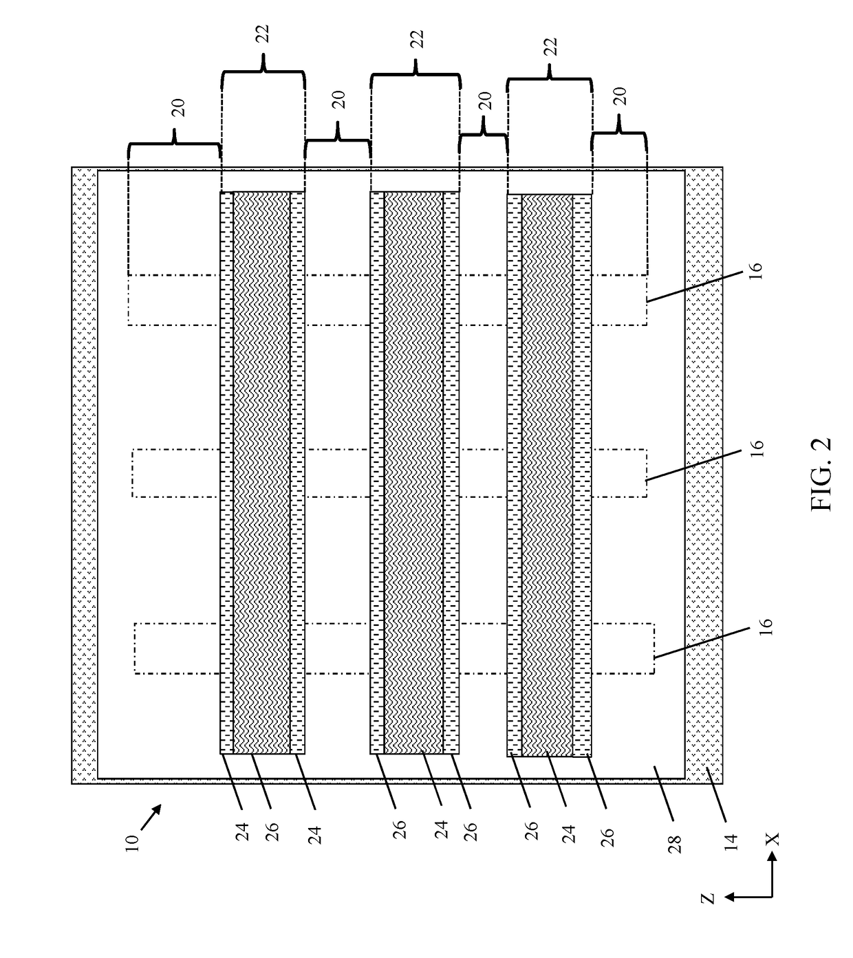
[0021]Embodiments of the present disclosure provide transistor structures for integrated circuits (ICs) to enhance manufacturability and performance. The present disclosure also contemplates methods for fabricating the transistor structure described herein. Generally, a transistor structure according to the present disclosure can include a semiconductor fin positioned on a substrate, and subdivided into two areas: a “gate area” dimensioned to have a first cross-sectional area, and a “terminal area” positioned laterally distal to the gate area and featuring a second cross-sectional area different from the first cross-sectional area. The gate area and terminal area of the semiconductor fin may otherwise have substantially identical material compositions. A transistor gate can be positioned on the first gate area of the semiconductor fin, while a contact can be positioned on the terminal area of the semiconductor fin. The differences in cross-sectional area throughout the semiconductor...


PUM


Abstract

Aspects of the present disclosure include finFET structures with varied cross-sectional areas and methods of forming the same. Methods according to the present disclosure can include, e.g., forming a structure including: a semiconductor fin positioned on a substrate, wherein the semiconductor fin includes: a gate area, and a terminal area laterally distal to the gate area, a sacrificial gate positioned on the gate area of the semiconductor fin, and an insulator positioned on the terminal area of the semiconductor fin; removing the sacrificial gate to expose the gate area of the semiconductor fin; increasing or reducing a cross-sectional area of the gate area of the semiconductor fin; and forming a transistor gate on the gate area of the semiconductor fin.

Description

FIELD OF THE INVENTION[0001]The subject matter disclosed herein relates to transistor structures with varied gate cross-sectional areas, and methods of fabricating the same. More specifically, aspects of the invention relate to finFET transistors in which a portion of a semiconductor fin, positioned beneath a gate, is shaped to have a greater or reduced cross-sectional area relative to laterally distal portions of the semiconductor fin.BACKGROUND[0002]In integrated circuit (IC) structures, a transistor is a critical component for implementing digital circuitry designs. Generally, a transistor includes three electrical terminals: a source, a drain, and a gate. By applying different voltages to the gate terminal, the flow of electric current between the source and the drain can be turned on and off. A common type of transistor is a metal oxide field effect transistor (MOSFET). One example of a MOSFET is a “FinFET,” typically formed upon a semiconductor-on-insulator (SOI) layer and bur...

Claims


Application Information

Patent Timeline
Patent Type & Authority Applications(United States)
IPC IPC(8): H01L29/66H01L29/423H01L21/768H01L21/306H01L21/324H01L29/78H01L21/321
CPCH01L29/66818H01L29/66545H01L29/785H01L21/76897H01L21/321H01L21/30604H01L21/324H01L29/42356H01L29/66795
Inventor SCHEPIS, DOMINIC J.REZNICEK, ALEXANDERKERBER, PRANITAOUYANG, QIQING C.
Owner GLOBALFOUNDRIES US INC
Why Eureka
Try Eureka