III-nitride heterojunction device

a heterojunction device and nitride technology, applied in the field of semiconductor devices, can solve the problems of large losses associated with resistance, large losses associated with charge, qg, qgd, etc., and achieve the effects of reducing the charge under the gate, reducing the gate area, and reducing the charg

Active Publication Date: 2008-12-04
INFINEON TECH AMERICAS CORP
View PDF7 Cites 4 Cited by
  • Summary
  • Abstract
  • Description
  • Claims
  • Application Information

AI Technical Summary

Benefits of technology

[0005]The invention disclosed here addresses a fundamental limitation to power management in the switch mode power supplies. Specifically, according to an aspect of the present invention, the gate charge is charged without changing the device gate width. More specifically, in a device according to the present invention, instead of reducing the charge under the gate to reduce the gate charge, the gate area is reduced by interrupting conduction under the gate which will reduce both the gate capacitance and conductivity with a smaller impact on resistance since the total ohmic contact area has not been affected. Furthermore, in a device according to the present invention, the size and the density of the ohmic contacts do not need to be adjusted as would be required when there is a blanket reduction of charge in the channel. Moreover, there will be no change in the threshold voltage of the device as may be the case when the charge is reduced in the entire region under the gate. Threshold voltage will not change since the charge density under the unaffected gate area has remained the same. Thus, the threshold voltage, gate charge, and device resistance can be tuned independently.
[0006]Advantageously, a process for fabricating a device according to the present invention will be easer compared to processes that require blanket gate charge density reduction. Moreover, the approach disclosed herein is dramatically reduces process influence on device characteristics.

Problems solved by technology

The losses associated with switch mode power supplies depend on the resistance of the FETs used in the circuit as well as the charge utilized by the driver during the switching event.
At higher frequencies, the losses associated with charge, Qg, Qgd, etc., become large, while at high currents, the losses associated with resistance becomes large.
The resistance of a device decreases with larger device width and smaller pitch (because of reduced channel and contact resistance), while the switching charge increases, which leads to a trade off between resistive and switching losses.
One strategy is to change the density of the two-dimensional gas (2-DEG) over the entire wafer during the formation of the III-nitride heterojunction, which leads to a penalty in drift resistance and associated RA product.
The current processes, such as gate recessing, are difficult to control.

Method used


Image

  • III-nitride heterojunction device
  • III-nitride heterojunction device
  • III-nitride heterojunction device

Examples


first embodiment

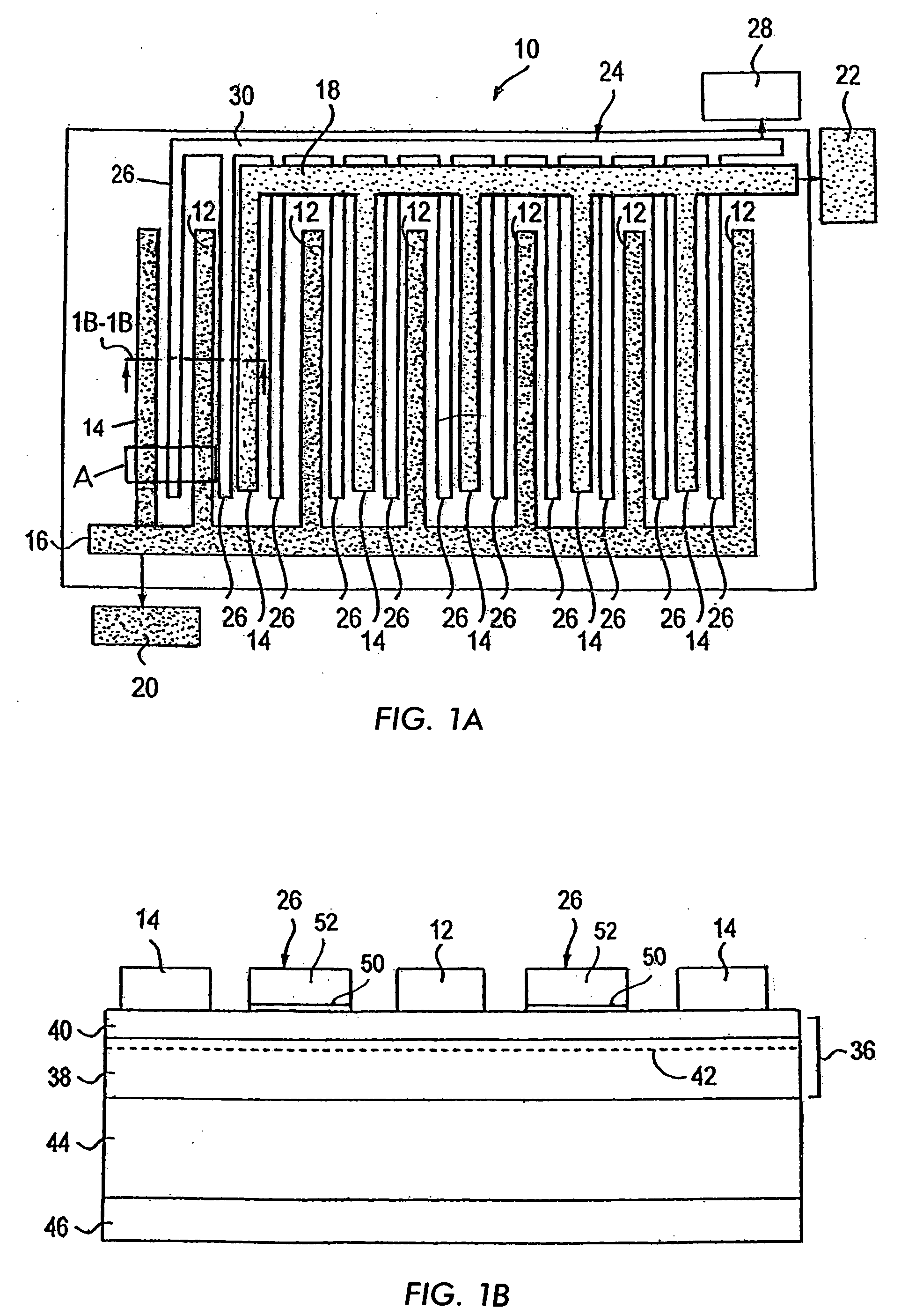
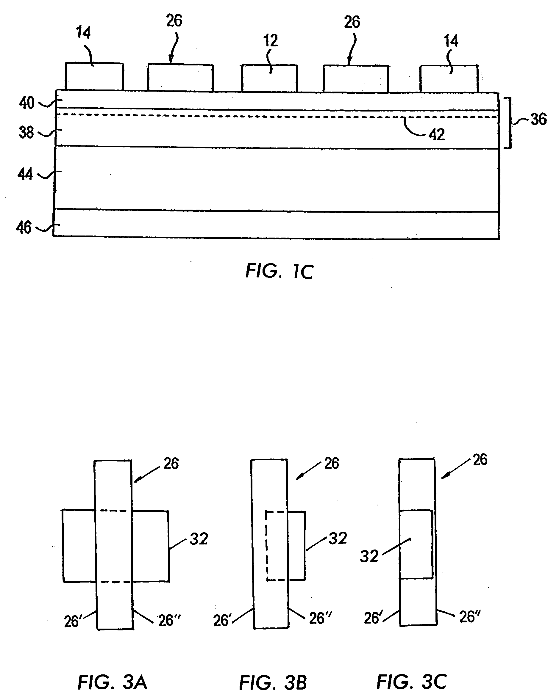
[0016]Referring to FIGS. 1A-1B, a power semiconductor device according to the present invention is a III-nitride based metal, insulator heterojunction field effect transistor (MISHFET) 10, which includes a plurality of first power electrodes (drain electrodes) 12, and a plurality of second power electrodes (source electrodes) 14 arranged in an interdigitated pattern. Drain electrodes 12 are electrically connected to one another by a respective drain feed 16 and source electrodes 14 are electrically connected to one another by a respective source feed 18. Drain feed 16 is also electrically connected to a first power pad (drain pad) 20 and source feed 18 is electrically connected to a second power pad (source pad) 22. Drain pad 20 and source pad 22 are located somewhere on the die and are used for external power connection.

[0017]Device 10 according to the first embodiment further includes a gate structure 24. Gate structure 24 includes a plurality of gate fingers 26 each disposed betw...

second embodiment

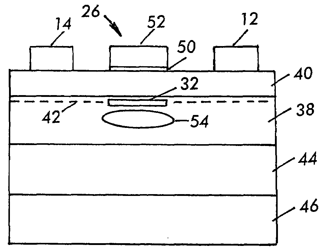
[0024]Referring now to FIG. 3A, in the present invention, at least one of the interrupted regions 32 may be wider than the width of and overlying gate finger 26. Thus, as illustrated by FIG. 3A, an interrupted region 32 can extend laterally beyond the lateral sides 26′, 26″ of a gate finger 26 that is disposed over the interrupted region 32.

[0025]Referring to FIG. 3B, in a third embodiment, an interrupted region 32 may extend only partially under a respective gate finger 26, while extending laterally beyond one of the lateral sides (e.g. side 26″) of the overlying gate finger 26. Referring to FIG. 3C, in a fourth embodiment of the present invention, an interrupted region 32 may extend only partially under a gate finger 26, but does not laterally extend beyond a lateral side (e.g. side 26′) of the overlying gate finger 26.

[0026]In any one of the embodiments disclosed herein, an interrupted region 32 may be formed by a recess 34 that partially extends through second III-nitride semico...


PUM


Abstract

A III-nitride heterojunction semiconductor device having a III-nitride heterojunction that includes a discontinuous two-dimensional electron gas under a gate thereof.

Description

RELATED APPLICATION[0001]This application is based on and claims priority to U.S. Provisional Application Ser. No. 60 / 931,339, filed on May 23, 2007, entitled Apertured Gate Channel for Gate Charge and RQ Reduction, to which a claim of priority is hereby made and the disclosure of which is incorporated by reference.DEFINITION[0002]III-nitride as used herein refers to a semiconductor alloy that includes nitrogen and a group III element such as Al, Ga, or In, including but not limited to AlN, GaN, AlGan, InGaN, InN, or InAlGaN.BACKGROUND AND SUMMARY OF THE INVENTION[0003]The present application relates to a semiconductor device.[0004]The losses associated with switch mode power supplies depend on the resistance of the FETs used in the circuit as well as the charge utilized by the driver during the switching event. At higher frequencies, the losses associated with charge, Qg, Qgd, etc., become large, while at high currents, the losses associated with resistance becomes large. The resis...

Claims


Application Information

Patent Timeline
Patent Type & Authority Applications(United States)
IPC IPC(8): H01L29/43
CPCH01L29/0692H01L29/1029H01L29/2003H01L29/7787H01L29/205H01L29/778
Inventor BRIDGER, PAULBEACH, ROBERT
Owner INFINEON TECH AMERICAS CORP
Why Eureka
Try Eureka