Lo generation and distribution in a multi-band transceiver

a multi-band transceiver and local oscillator technology, applied in the direction of digital transmission, pulse automatic control, wireless commuication services, etc., can solve the problems of high cost of implementation, disturbance of vco, and low current consumption, and achieve low cost, small current consumption, and reasonable power consumption and reliability

Active Publication Date: 2012-05-17
QUALCOMM INC
View PDF7 Cites 30 Cited by
  • Summary
  • Abstract
  • Description
  • Claims
  • Application Information

AI Technical Summary

Benefits of technology

[0013]An on-chip internal test loop back connection is also provided. This test loop back connection allows the receiver on the chip for the second frequency band to receive and detect a signal output by the transmitter on the chip for the second frequency band. After the loop back signal has been received in this way and has been demodulated, evidence of phase mismatch in the components of the quadrature LO signals of the transmitter and / or receiver is detected. The first phase mismatch correction circuits in the quadrature LO signal paths going to the transmitter and / or receiver are then controlled so that the relative phases of the component signals are adjusted such that the detected phase mismatch is reduced or eliminated.
[0016]The coupling gain of signals into the tank of the VCO is made to drop off rapidly for signals above ten gigahertz so that any harmonics of Power Amplifier (PA) output signals above ten gigahertz will not unduly perturb VCO operation. Even order harmonics of the 5.0 GHz and 2.5 GHz PA output signals may land on the ten gigahertz operating frequency of the VCO, but they have little impact on VCO operation due to their relative low strengths (as compared to the signal strengths of odd order harmonics) and due to the differential nature of the routing circuitry. As compared to offset LO architecture of the prior art and as compared to the heterodyne LO architecture of the prior art, the novel LO generation and distribution circuitry described above can be realized in a comparatively small amount of integrated circuit area and can be made to have a comparatively small current consumption.

Problems solved by technology

Unfortunately, a strong transmitter output signal from a PA can be injected back such that it disturbs the VCO if the VCO is operating at the same approximate frequency as the PA output signal frequency.
This simple architecture is generally not used because it has a very high power consumption due to parasitics in the routing and because it suffers from reliability and yield problems due to the high frequency of operation in the LO distribution network.
This offset LO architecture, however, has drawbacks in that it is expensive to implement.
It also exhibits fairly high current consumption.
These two drawbacks make it undesirable for use in a cellular handset application.
Unfortunately, the heterodyne LO architecture of FIG. 2 is also expensive to implement and has a relatively large current consumption.
A further drawback is that signal quality may be compromised due to additional unwanted tones generated by the additional mixing circuitry involved.

Method used


Image

  • Lo generation and distribution in a multi-band transceiver
  • Lo generation and distribution in a multi-band transceiver
  • Lo generation and distribution in a multi-band transceiver

Examples


Embodiment Construction

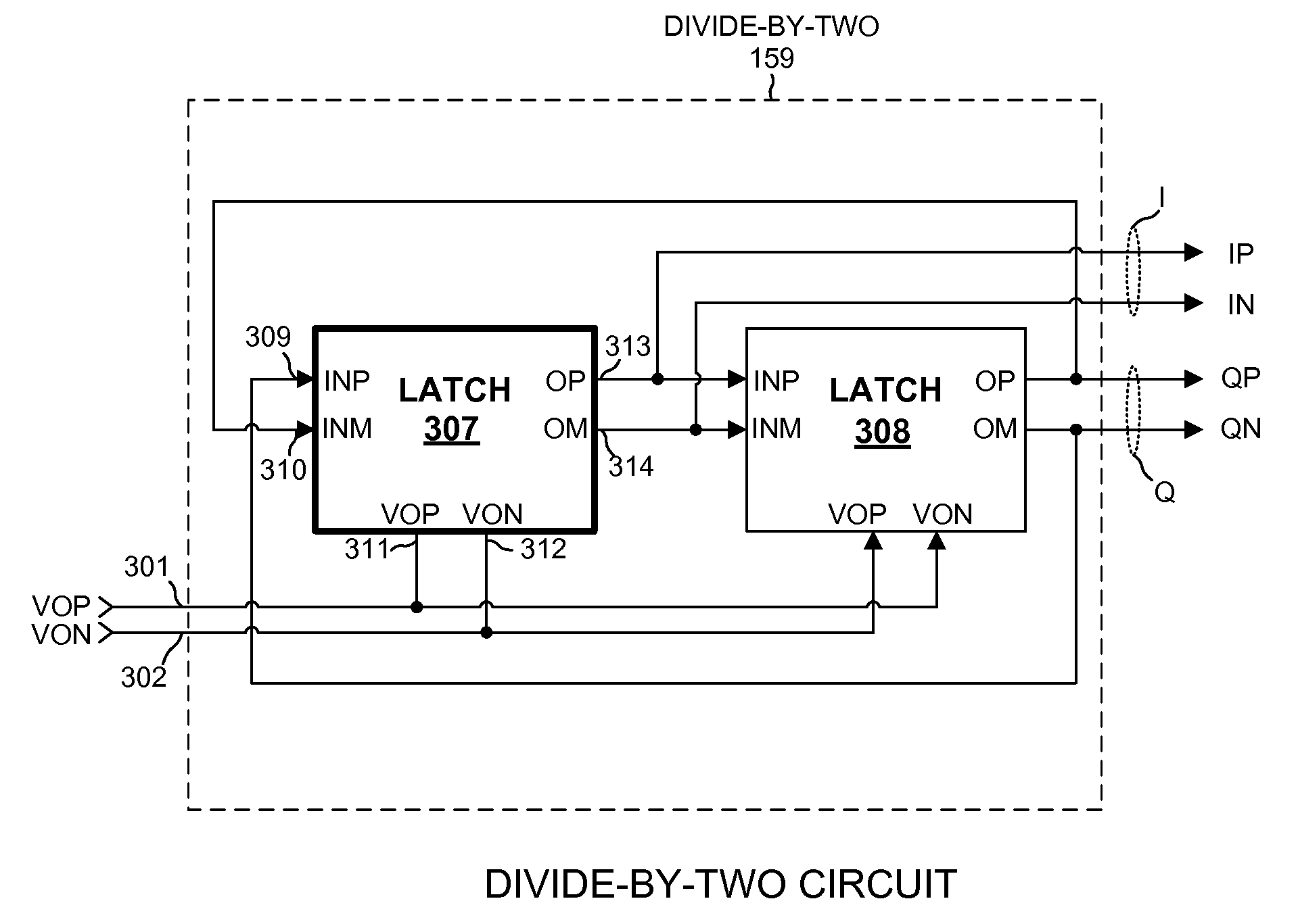
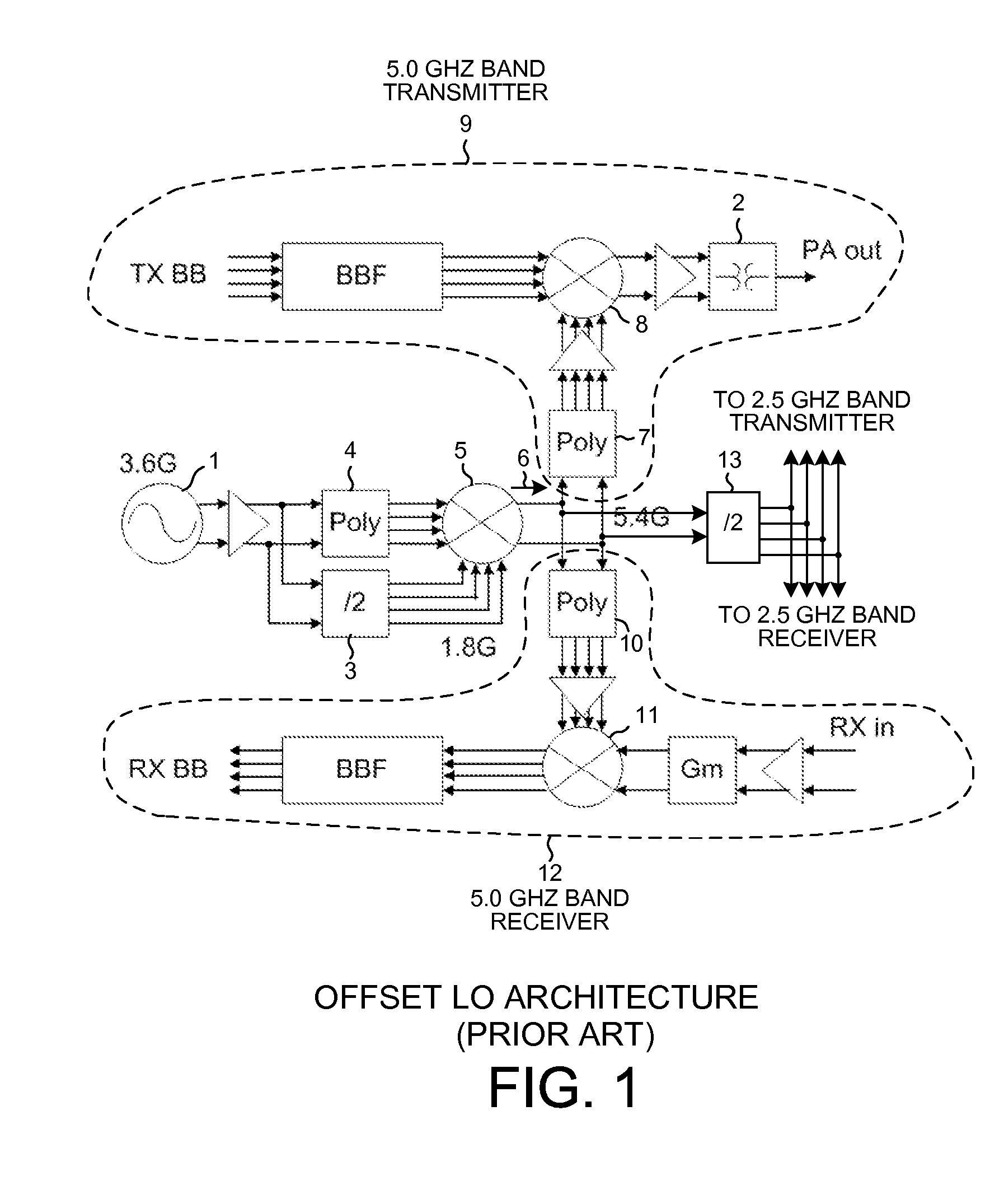
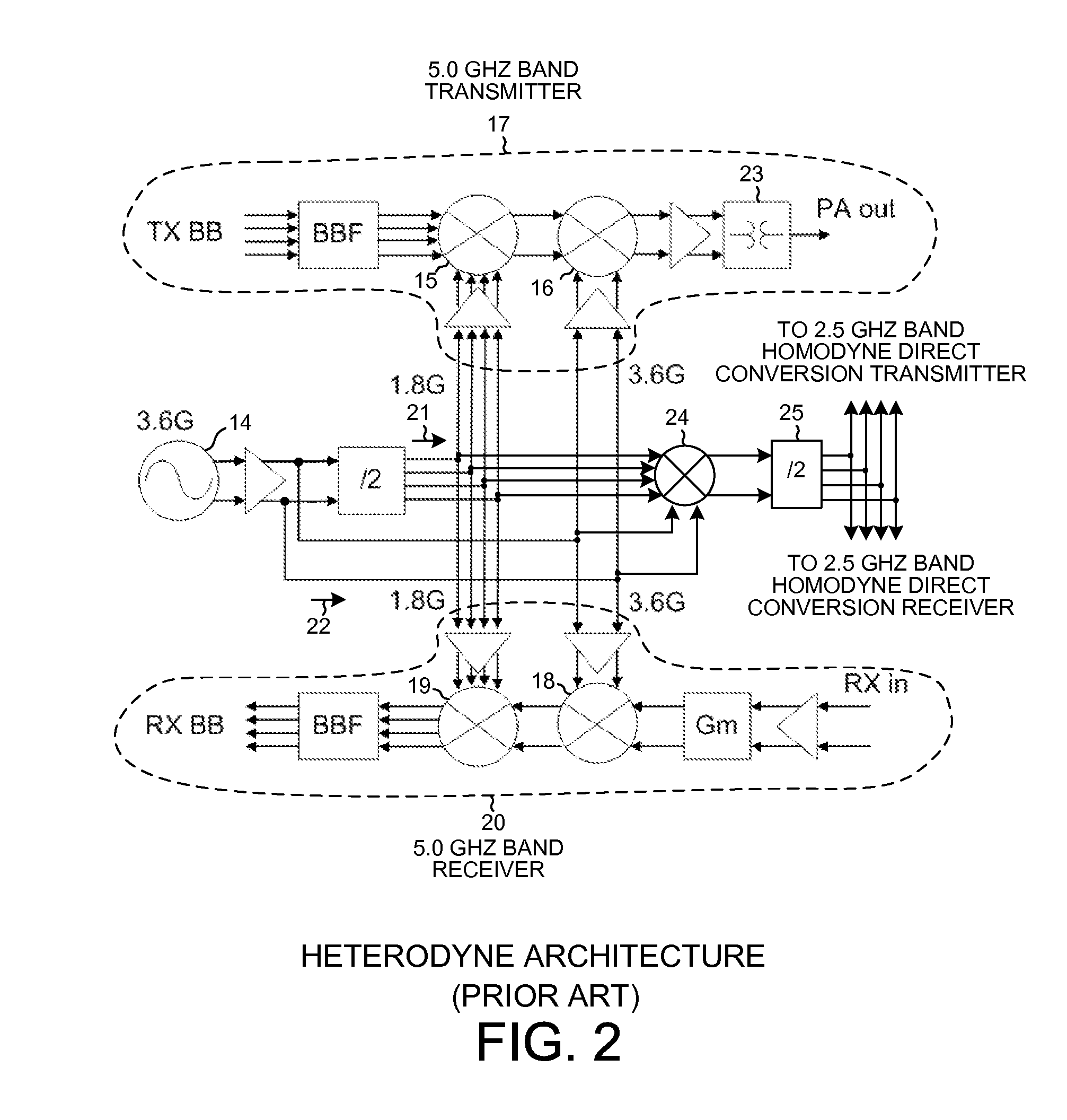
[0037]FIG. 3 is a diagram of a multi-band IEEE802.11 mobile station device (STA) 100 transceiver embodied in a cellular telephone handset. The IEEE802.11 transceiver is called “multi-band” in that it can operate in accordance with the IEEE802.11a standard using a frequency band from 4.915 GHz to 5.825 GHz or it can operate in accordance with the IEEE802.11b / g standard using a frequency band from 2.412 GHz to 2.484 GHz. For simplification purposes, the lower band from 2.412 GHz to 2.484 GHz band is referred to hereinafter as the “first frequency band” and the higher band from 4.915 GHz to 5.825 GHz is referred to hereinafter as the “second frequency band”. IEEE802.11b / g is referred to as the “first standard”. IEEE802.11a is referred to as the “second standard”. Transceiver 100 includes (among other parts not illustrated) an antenna 101, an RF transceiver integrated circuit 102, and a digital baseband integrated circuit 103. RF transceiver integrated circuit 102 is called a “transceiv...


PUM


Abstract

A VCO of a PLL outputs a first differential signal of frequency FVCO. A first divide-by-two circuit local to the VCO divides the first differential signal and outputs a first quadrature signal of frequency FVCO / 2. Two of the component signals of the first quadrature signal are routed to a second divide-by-two circuit local to a first mixer of a first device. The second divide-by-two circuit outputs a second quadrature signal of frequency FVCO / 4 to the first mixer. All four signals of the first quadrature signal of frequency FVCO / 2 are routed through phase mismatch correction circuitry to a second mixer of a second device. In one example, FVCO is a tunable frequency of about ten gigahertz, the first device is an IEEE802.11b / g transmitter or receiver that transmits or receives in a first band, and the second device is an IEEE802.11a transmitter or receiver that transmits or receives in a second band.

Description

BACKGROUND[0001]1. Technical Field[0002]The present disclosure relates to the generation and distribution of local oscillator signals within a multi-band transceiver.[0003]2. Background Information[0004]Cellular telephone handsets are sometimes made to have a multi-band WiFi communication capability where the WiFi communication capability is to be compliant with multiple Institute of Electrical and Electronic Engineers (IEEE) standards including IEEE802.11a, IEEE802.11b, and IEEE802.11g. Due to the application in a cellular telephone handset, reducing the integrated circuit area consumed by the multi-band transceiver is important to reduce cost. Maintaining low power consumption is also important to increase talk time. If the multi-band transceiver is to operate in compliance with the IEEE802.11b and IEEE802.11g standards, then it should be able to receive and to transmit signals in the so-called 2.5 GHz band. This band actually extends from a lower bound of approximately 2.412 GHz ...

Claims


Application Information

Patent Timeline
Patent Type & Authority Applications(United States)
IPC IPC(8): H04B1/40H04W40/00
CPCH03L7/099H03L7/104H03L7/16H04B1/40H03L7/1976H04B1/0082H03L7/193H04B1/00
Inventor SOLTANIAN, BABAKSAVOJ, JAFAR
Owner QUALCOMM INC
Why Eureka
Try Eureka