Display substrate, method of manufacturing the display substrate and display device having the display substrate

a technology of display substrate and manufacturing method, which is applied in the direction of non-linear optics, instruments, optics, etc., can solve the problems of image display quality decline, and achieve the effects of reducing the area of contact holes, reducing the distance interval, and reducing the area of gate metal patterns

Active Publication Date: 2010-01-28
SAMSUNG DISPLAY CO LTD
View PDF1 Cites 13 Cited by
  • Summary
  • Abstract
  • Description
  • Claims
  • Application Information

AI Technical Summary

Benefits of technology

[0026]In an exemplary embodiment of the present invention, the display device may further include a voltage-decreasing groove aligned with the voltage-decreasing electrode so as to reduce a distance interval between the voltage-decreasing electrode and the voltage-decreasing line.
[0027]According to the present invention, a storage-down voltage is directly applied to a voltage-decreasing line which is a transparent metal pattern. Thus, the area of gate metal patterns may be reduced, and the area of contact holes may be reduced; thus, the aperture ratio may be improved.

Problems solved by technology

As a result, image display quality may be decreased.

Method used


Image

  • Display substrate, method of manufacturing the display substrate and display device having the display substrate
  • Display substrate, method of manufacturing the display substrate and display device having the display substrate
  • Display substrate, method of manufacturing the display substrate and display device having the display substrate

Examples


exemplary embodiment 1

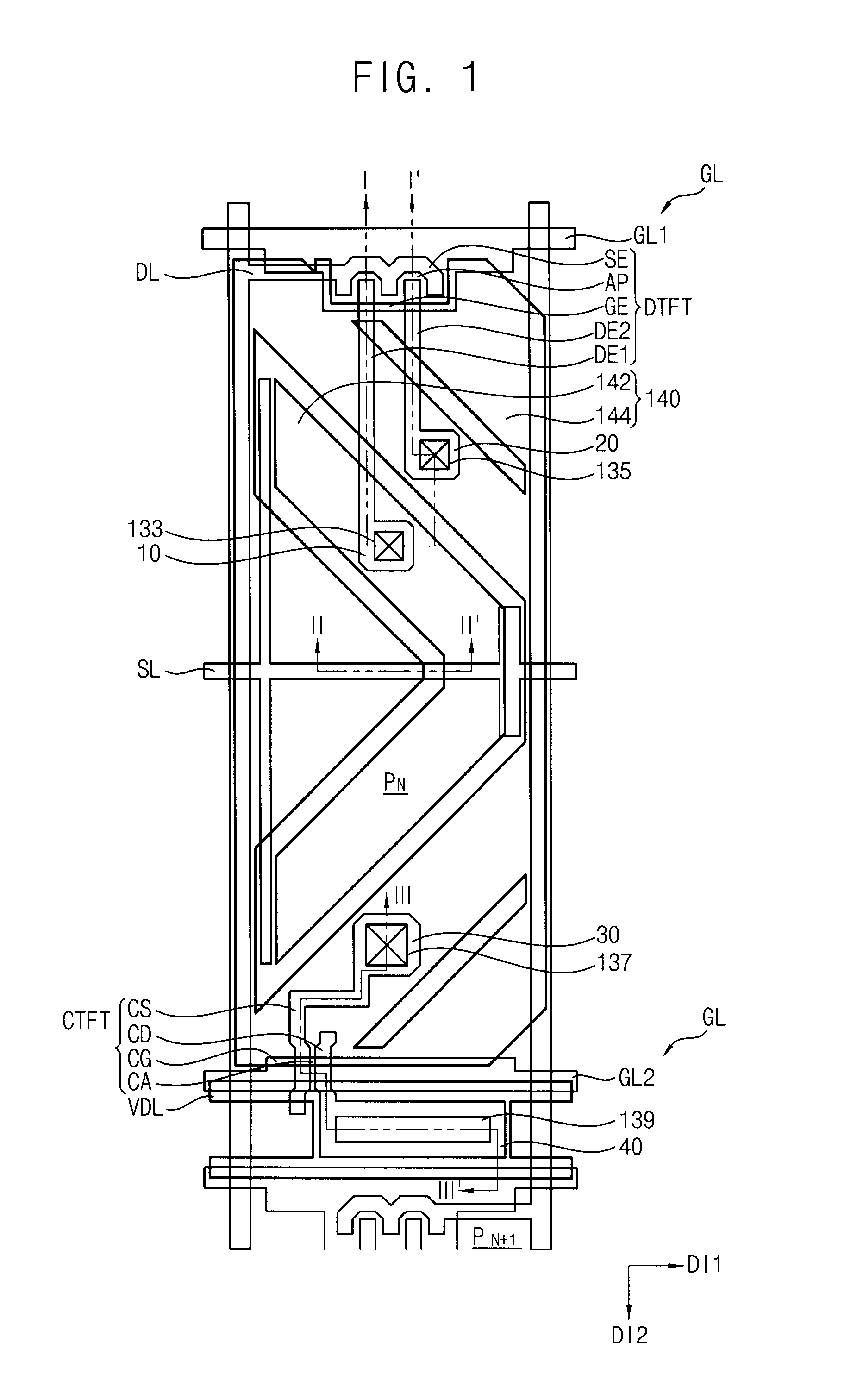
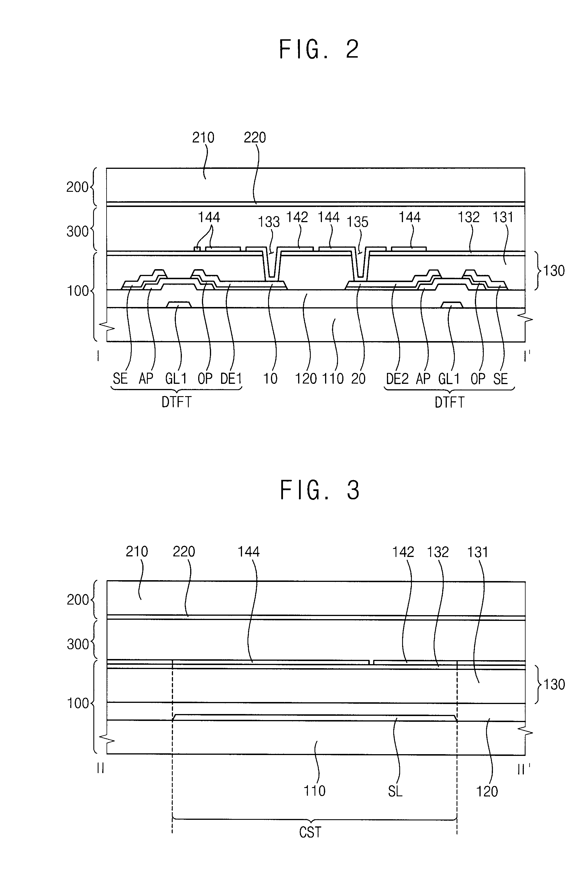
[0044]FIG. 1 is a top plan view illustrating an exemplary embodiment of a unit pixel of a first exemplary embodiment of a display device according to the present invention. FIG. 2 is a cross-sectional view taken along line I-I′ in FIG. 1. FIG. 3 is a cross-sectional view taken along line II-II′ in FIG. 1. FIG. 4 is a cross-sectional view taken along line III-III′ in FIG. 1.

[0045]Referring to FIGS. 1 to 4, the first exemplary embodiment of a display device according to the present invention includes a first substrate 100, a second substrate 200 facing the first substrate 100, and a liquid crystal layer 300 interposed between the first and second substrates 100 and 200.

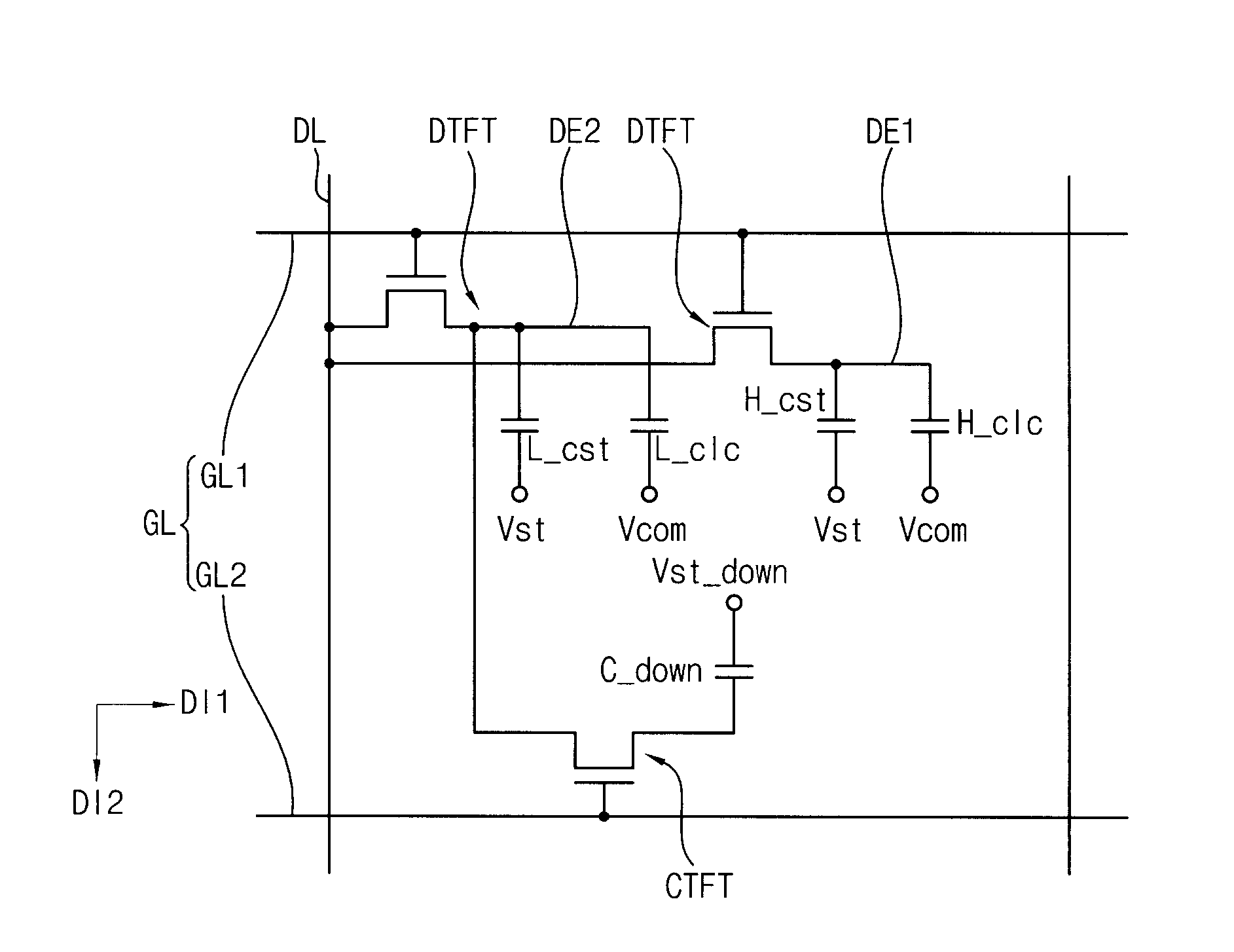
[0046]In the present exemplary embodiment, the first substrate 100 may include a first transparent substrate 110, a plurality of gate lines GL, a plurality of storage lines SL, a gate insulation layer 120, a plurality of voltage-decreasing lines VDL, a plurality of data lines DL, a data insulation layer 130, a plurality...

exemplary embodiment 2

[0109]FIG. 7 is a cross-sectional view illustrating an exemplary embodiment of a unit pixel of a second exemplary embodiment of a display device according to the present invention. A top plan layout view illustrating a unit pixel of the second exemplary embodiment of a display device according to the present invention is substantially the same as that of the first exemplary embodiment of a display device according to the present invention, except that the organic insulation layer 131 is formed on the inorganic insulation layer 132 and the voltage-decreasing lines VDL occasionally directly contacts the organic insulation layer 131. Additionally, a cross-sectional view taken along a line I-I′ in FIG. 1, and a cross-sectional view taken along a line II-II′ in FIG. 1 according to the second exemplary embodiment of the present invention are substantially the same as that of the first exemplary embodiment of a display device according to the present invention. Thus, corresponding referenc...


PUM

PropertyMeasurementUnit
voltageaaaaaaaaaa
transparentaaaaaaaaaa
lengthaaaaaaaaaa

Abstract

A display substrate includes; a dual transistor electrically connected to a first gate line and a data line, which is disposed in a direction substantially perpendicular to the first gate line, the dual transistor including a first drain electrode and a second drain electrode, a pixel electrode having a first pixel part and a second pixel part which are respectively connected to the first drain electrode and the second drain electrode, a connection transistor electrically connected to the second pixel part and a second gate line which is adjacent to the first gate line, the connection transistor comprising a connection drain electrode, a voltage-decreasing electrode extended from a connection drain electrode of the connection transistor a voltage-decreasing line extended in substantially the same direction as the first and second gate lines, and disposed on a data insulation layer overlapping the voltage-decreasing electrode and the data insulation layer.

Description

[0001]This application claims priority to Korean Patent Application No. 2008-71425, filed on Jul. 23, 2008, and all the benefits accruing therefrom under 35 U.S.C. §119, the contents of which in its entirety are herein incorporated by reference.BACKGROUND OF THE INVENTION[0002]1. Field of the Invention[0003]Exemplary embodiments of the present invention relate to a display substrate, a method of manufacturing the display substrate, and a display device having the display substrate. More particularly, exemplary embodiments of the present invention relate to a display substrate having an enhanced viewing angle and an improved aperture ratio, a method of manufacturing the display substrate, and a display device having the display substrate.[0004]2. Description of the Related Art[0005]Generally, a liquid crystal display (“LCD”) device includes a first substrate having a pixel electrode formed in a unit pixel, a second substrate having a common electrode facing the first substrate, and a...

Claims


Application Information

Patent Timeline
Patent Type & Authority Applications(United States)
IPC IPC(8): G02F1/1368G02F1/13
CPCG02F2001/134345G02F1/13624G02F1/134345G02F1/1343G02F1/136
Inventor PARK, KEE-BUMCHO, EUNKIM, DONG-GYU
Owner SAMSUNG DISPLAY CO LTD
Why Eureka
Try Eureka