Nonvolatile memory device and method for fabricating the sam

a memory device and non-volatile technology, applied in the direction of semiconductor devices, electrical devices, transistors, etc., can solve the problems of difficult fabrication of memory devices by process technology under 40 nm, and cannot cope with the decrease of a design rule of the device, so as to increase the effective channel width, reduce the gate area, and high the effect of memory device integration

Inactive Publication Date: 2009-01-08
SK HYNIX INC
View PDF22 Cites 6 Cited by
  • Summary
  • Abstract
  • Description
  • Claims
  • Application Information

AI Technical Summary

Benefits of technology

[0007]To overcome the above-mentioned problems, this invention provides a nonvolatile memory device and a method for fabricating the same by increasing an effective channel width to cope with decrease of a gate area due to the high integration of the memory device, thereby securing an operation current.

Problems solved by technology

However, it can not actually cope with the decrease of a design rule of the device.
However, a memory device fabricated by a process technology of 40 nm or less has problems such as an interference and a disturbance, i.e., a phenomenon that a threshold voltage of a neighboring cell changes during program operation of a cell, and thus it is difficult to fabricate the memory device by a process technology under 40 nm.

Method used


Image

  • Nonvolatile memory device and method for fabricating the sam
  • Nonvolatile memory device and method for fabricating the sam
  • Nonvolatile memory device and method for fabricating the sam

Examples


Embodiment Construction

[0016]Embodiments of the present invention relate to a method for a nonvolatile memory device and a method for fabricating the same.

[0017]Referring to the drawings, the illustrated thickness of layers and regions are exaggerated to facilitate explanation. When a first layer is referred to as being “on” a second layer or “on” a substrate, it could mean that the first layer is formed directly on the second layer or the substrate, or it could also mean that a third layer may exist between the first layer and the second layer or the substrate. Furthermore, the same or like reference numerals throughout the various embodiments of the present invention represent the same or similar elements in different drawings.

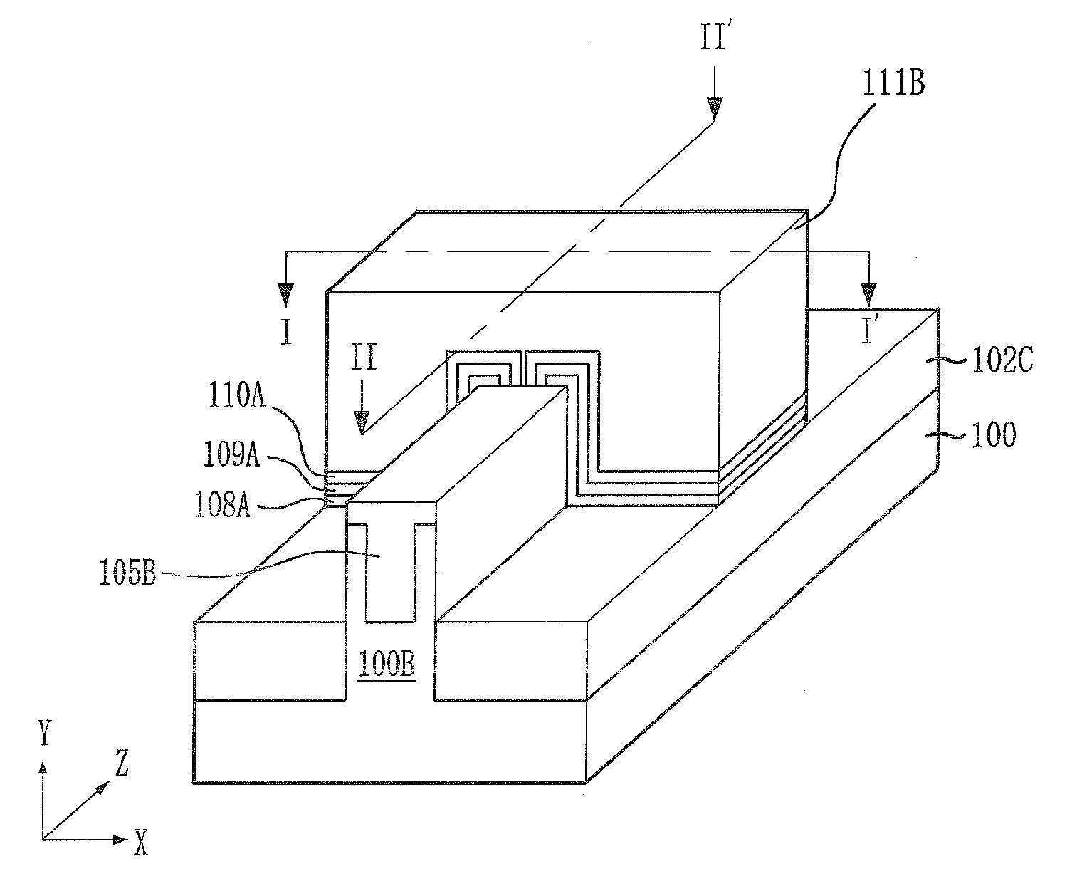
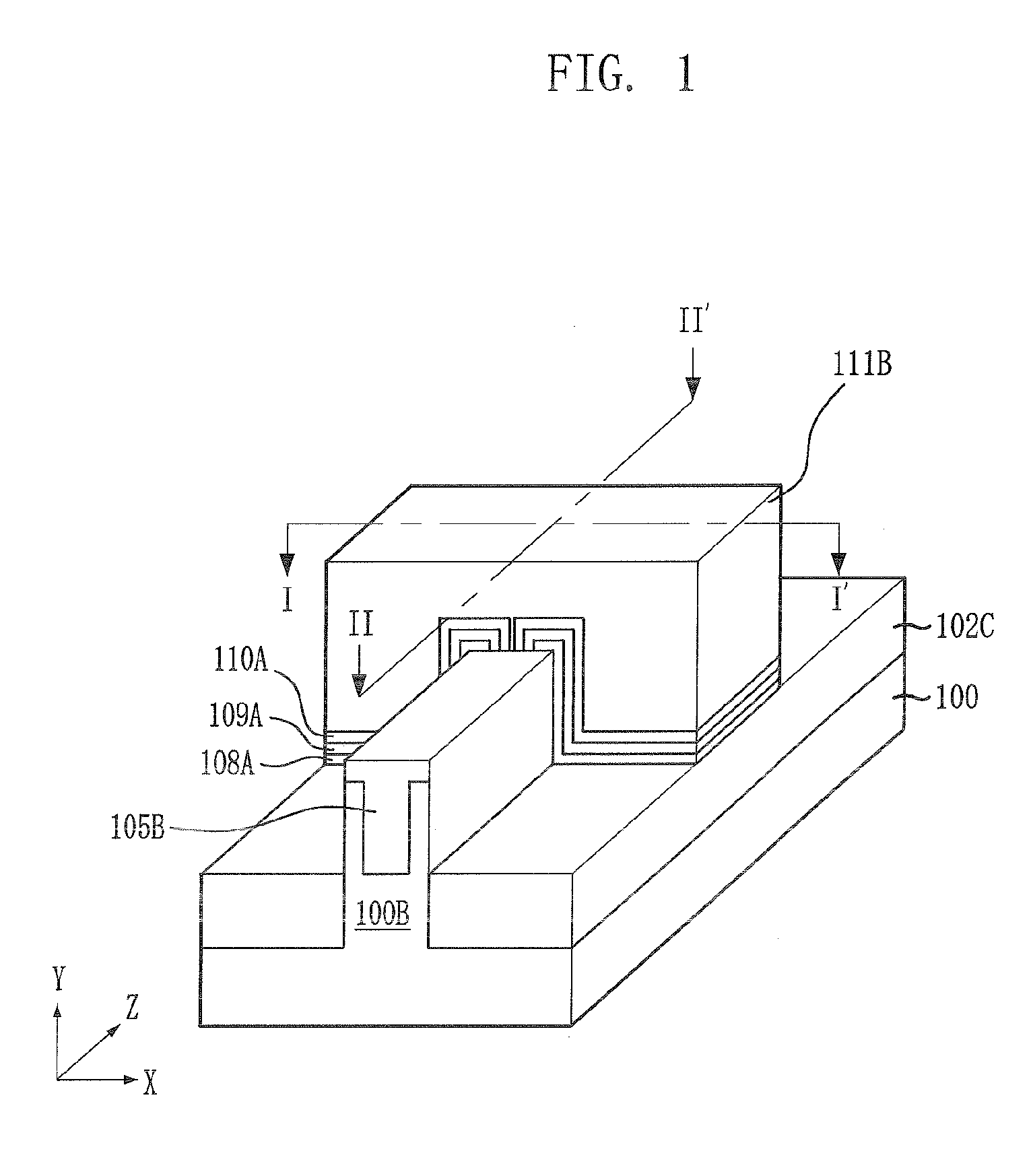
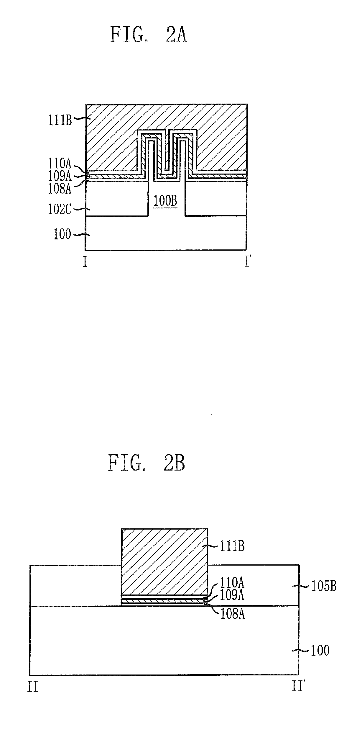
[0018]FIG. 1 is a perspective view of a floating trap type memory device, i.e., a memory device for storing an electric charge in an insulating charge storage layer formed between a gate electrode and a substrate, illustrating a nonvolatile memory device in accordance with an embo...


PUM


Abstract

A nonvolatile memory device includes an active region which is defined by an isolation layer formed in a substrate and has a recess therein in a channel width direction, wherein an upper portion of the active region having the recess projects over an upper portion of the isolation layer, a lower insulation layer formed along a surface of the active region and a top surface of the isolation layer, a charge storage layer formed over the lower insulation layer, an upper insulation layer formed over the charge storage layer, and a gate electrode formed over the upper insulation layer.

Description

CROSS-REFERENCE TO RELATED APPLICATIONS[0001]The present invention claims priority to Korean patent application number 2007-0066169, filed on Jul. 2, 2007, which is incorporated by reference in its entirety.BACKGROUND OF THE INVENTION[0002]The present invention relates to a nonvolatile memory device and a method for fabricating the same, and more particularly, to a unit cell in a nonvolatile memory device including a multi-channel for storing data and a method for fabricating the same.[0003]Recently, there has been increased demand for nonvolatile memory devices which can be electrically programmed and erased and do not perform a refresh operation for periodically re-writing data unlike a volatile memory device, thereby achieving low power consumption. To develop a mass storage memory device, research is in progress for fabricating a highly integrated nonvolatile memory device.[0004]Demand for a flash memory device which belongs to the nonvolatile memory devices has been increased. ...

Claims


Application Information

Patent Timeline
Patent Type & Authority Applications(United States)
IPC IPC(8): H01L29/792H01L29/788H01L21/336
CPCH01L21/28273H01L21/28282H01L29/792H01L29/66833H01L29/7881H01L29/66825H01L29/40114H01L29/40117H01L21/28141H01L21/76838
Inventor LEE, SEUNG-CHEOLJANG, CHUL-SIK
Owner SK HYNIX INC
Why Eureka
Try Eureka