
Method for forming active region and semiconductor device
An active area and substrate technology, applied in semiconductor/solid-state device manufacturing, electrical components, circuits, etc., can solve the problem of no solution, low bonding force between the isolation dielectric layer and the shallow trench, and the inability to increase the effective trench of the active device. channel width and other issues, to achieve the effect of increasing the effective channel width, improving the bonding force is not high, and improving the isolation effect
Patent Information
- Authority / Receiving Office
- CN · China
- Patent Type
- Patents(China)
- Current Assignee / Owner
- Publication Date
- 2018-07-20
Smart Images
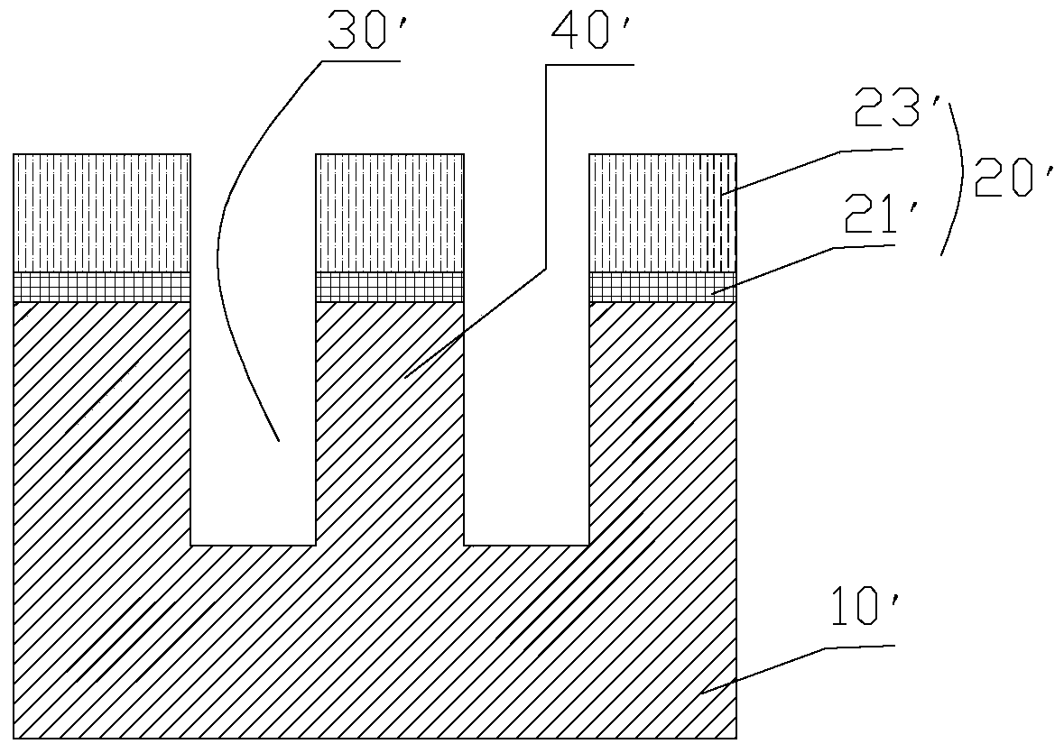
Figure 1 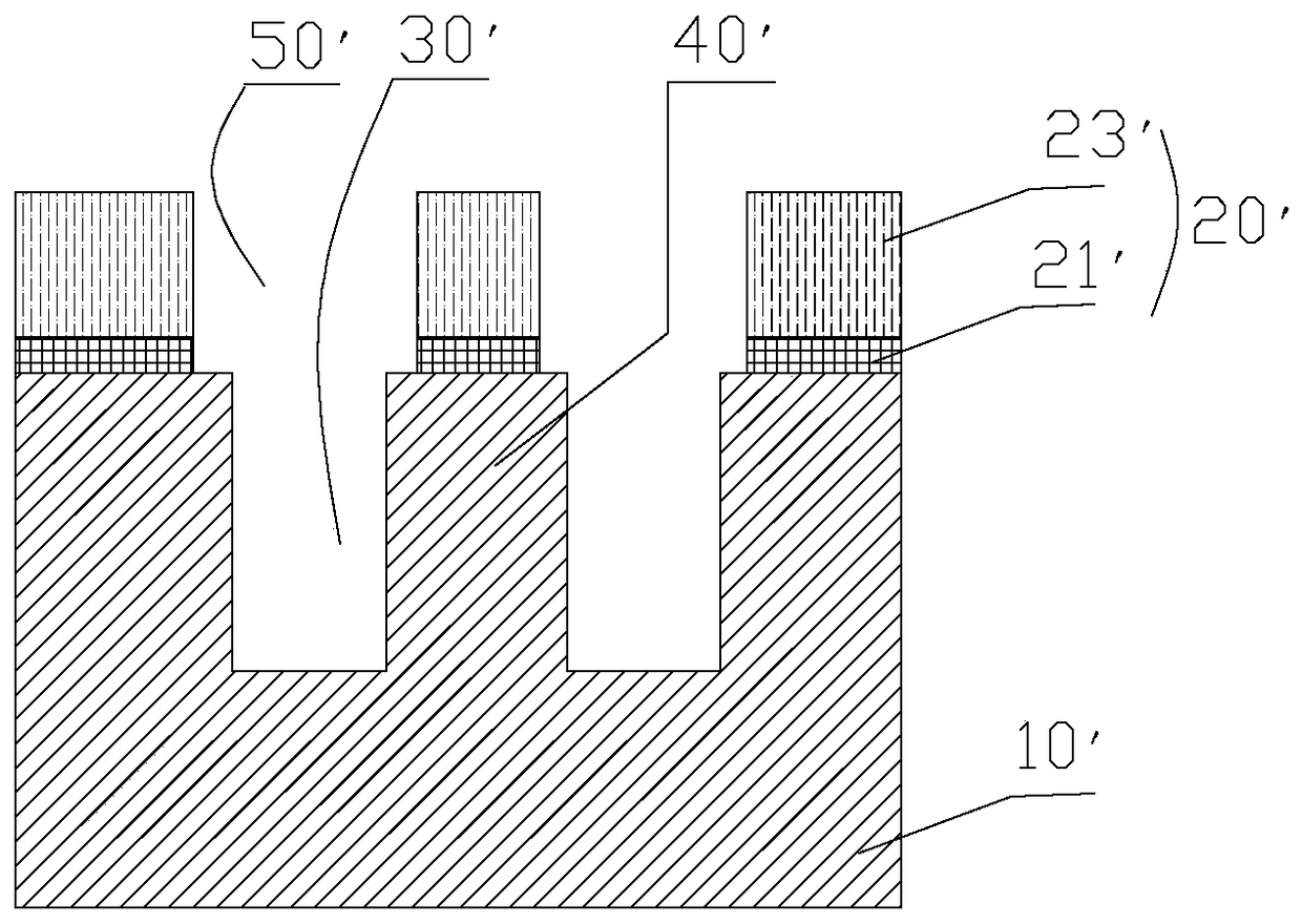
Figure 2 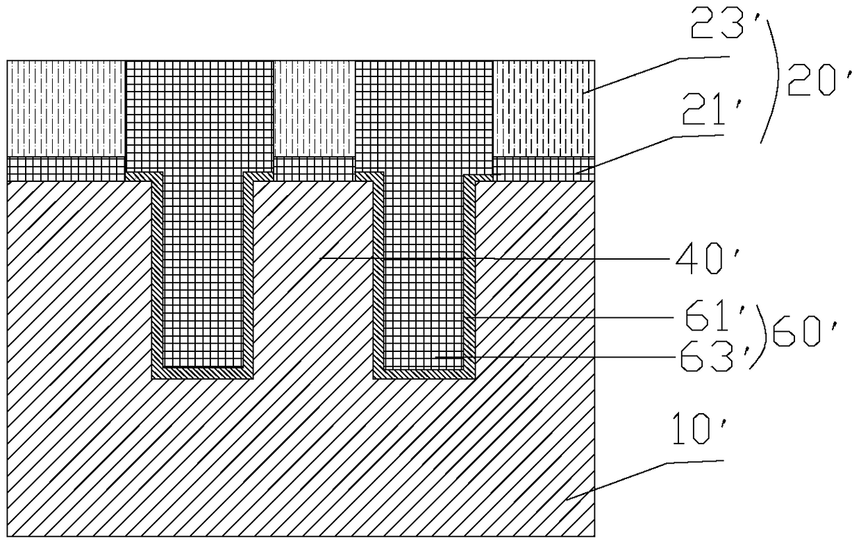
Figure 3
Abstract
Description
technical field
[0001] The invention relates to a manufacturing process of a semiconductor integrated circuit, in particular to a method for forming an active region and a semiconductor device. Background technique
[0002] In the manufacturing process of semiconductor devices, it is necessary to define the position of the active region in the substrate, and then form active devices such as transistors in the active region. When the active device is in the working state, a conductive channel is formed in the active region, and as the length of the conductive channel decreases or the width of the conductive channel increases, the operating current of the active device increases accordingly. At present, shallow trench isolation technology (Shallow Trench Isolation, STI) is usually used to define the position of the active region, that is, a trench isolation structure is formed in the substrate, and the substrate between adjacent trench isolation structures is used as the activ...
Examples
Embodiment Construction
[0031] The technical scheme of the present application will be described in detail below in conjunction with the specific implementation of the present application, but the following examples are only used to understand the present application, and cannot limit the present application. The embodiments in the present application and the features in the embodiments Combinable with each other, the application can be implemented in many different ways as defined and covered by the claims.
[0032] It can be seen from the background art that the active region formed by the existing method has nearly right-angled corners, so that the effective channel width of the active device cannot be increased, and the operating current of the active device cannot be increased. The inventors of the present application conducted research on the above problems and proposed a method for forming an active region. Such as Figure 5 As shown, the method includes the following steps: forming a base st...