Manufacturing method of semiconductor device

A manufacturing method and semiconductor technology, which is applied in semiconductor/solid-state device manufacturing, semiconductor devices, electric solid-state devices, etc., can solve the problems such as repeated erasing times index is not up to standard, so as to improve the speed and performance of the device and increase the conduction current , The effect of saving process cost

Active Publication Date: 2021-05-25
WUHAN XINXIN SEMICON MFG CO LTD
View PDF5 Cites 0 Cited by
  • Summary
  • Abstract
  • Description
  • Claims
  • Application Information

AI Technical Summary

Problems solved by technology

If the identification window is too small, the repeated erasure index of the next-generation technology t-1 will not meet the standard. Therefore, without increasing the size of the device, in order to maintain the key performance of the next-generation technology t-1 to maintain the key performance of the previous generation technology t indicators, increasing the on-current Idsat of the memory cell becomes a key factor

Method used


Image

  • Manufacturing method of semiconductor device
  • Manufacturing method of semiconductor device
  • Manufacturing method of semiconductor device

Examples


Embodiment Construction

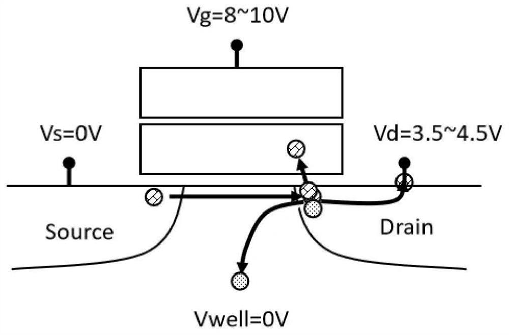
[0045] Transistor conduction current principle:

[0046]

[0047] In the formula, Idsat is the conduction current, Cox is the parasitic capacitance, μ is a constant, W is the effective channel width, L is the effective channel length, V GS is the gate-source voltage difference, VT is the threshold voltage.

[0048] It can be seen from the above formula that the conduction current Idsat of the transistor is inversely proportional to the effective channel length L and directly proportional to the effective channel width W.

[0049] As mentioned in the background art, the logic circuit has evolved all the way to the current 5nm process, which is mainly to reduce the effective channel length L of the MOS transistor and increase the speed of the logic circuit.

[0050] However, the conduction current Idsat of the transistor is also proportional to the effective channel width W, so the conduction current can be increased by increasing the effective channel width W at this time. ...


PUM


Abstract

The invention provides a method for manufacturing a semiconductor device. After using a mask layer to etch a semiconductor substrate to form an active region, the line width of the mask layer is gradually reduced, and the exposed area of ​​the mask layer is The top surface of the active region is trimmed into an arc-shaped surface, the longitudinal section of the arc-shaped surface is between an elliptical arc and a circular arc, and its maximum ideal value can be a circular arc. At this time, when the existing design rules define When the line width of the active region is A, the surface arc length corresponding to the curved surface of the improved active region of the present invention is between A and 3.14A, and the effective channel width is significantly increased. According to the conduction current In direct proportion to the effective channel width, the conduction current of the device is significantly increased, thereby effectively improving the speed and performance of the device. In addition, after trimming the top surface of the active region into an arc-shaped surface, the mask layer is still retained, so that the mask layer can be used to open the insulating isolation layer later, thereby simplifying the process and saving costs.

Description

technical field [0001] The invention relates to the technical field of manufacturing semiconductor devices, in particular to a method for manufacturing semiconductor devices. Background technique [0002] The technical development of planar semiconductor devices follows Moore's Law, and lower power consumption and higher speed have become the main theme of the current planar semiconductor device technology development. For logic circuits, the conduction current of MOS transistors is inversely proportional to its effective channel length, so the way to increase the speed of logic circuits is usually to reduce the effective channel length of MOS transistors, thus, logic circuits have evolved all the way to today's 5 nanometers craft. [0003] Take code flash memory as an example, please refer to figure 1 As shown, the programming (Program) of the code type flash memory is realized by hot electron injection (Hot Electron Injection). Specifically, when programming, a voltage V...

Claims


Application Information

Patent Timeline
Patent Type & Authority Patents(China)
IPC IPC(8): H01L27/11517H01L27/11521H01L21/308
CPCH01L21/3083H01L21/3085H10B41/00H10B41/30
Inventor 杨道虹周俊孙鹏
Owner WUHAN XINXIN SEMICON MFG CO LTD
Why Eureka
Try Eureka