
Semiconductor power device

a technology of magnetic field and power device, which is applied in the direction of magnetic field device, basic electric element, electrical apparatus, etc., can solve the problems of reducing the channel mobility, affecting the short circuit withstanding time of devices, and much higher channel resistance, so as to reduce specific on-resistance (ron,sp), the effect of increasing the channel width density

Active Publication Date: 2019-03-14
SHANGHAI HESTIA POWER INC
View PDF2 Cites 1 Cited by
  • Summary
  • Abstract
  • Description
  • Claims
  • Application Information

AI Technical Summary

Benefits of technology

The present invention aims to improve the on-resistance of a semiconductor power device. This is achieved by increasing the channel width density, which reduces the specific on-resistance for a given area. Additionally, the invention allows for a higher channel width density without changing the design rule by using a tighter design rule for the distance between the source contact and the gate electrode and by forming channels at both sides of the arms. These improvements in the invention enhance the efficiency and reliability of semiconductor power devices.

Problems solved by technology

When a gate dielectric is formed in a silicon carbide MOSFET by thermal oxidation, unreacted carbon may remain at the interface between the gate dielectric and the silicon carbide to form defects such as silicon vacancy, carbon clusters or carbon interstitial, these defects create energy states within the band gap and become acceptor traps or donor traps.
These two effects significantly reduce the channel mobility of SiC MOSFET and result in a much higher channel resistance compared to SiC MOSFET.
However, reducing the channel length Lch will increase the saturation current of MOSFET due to short channel effect, which will adversely impact the short circuit withstanding time of devices.

Method used

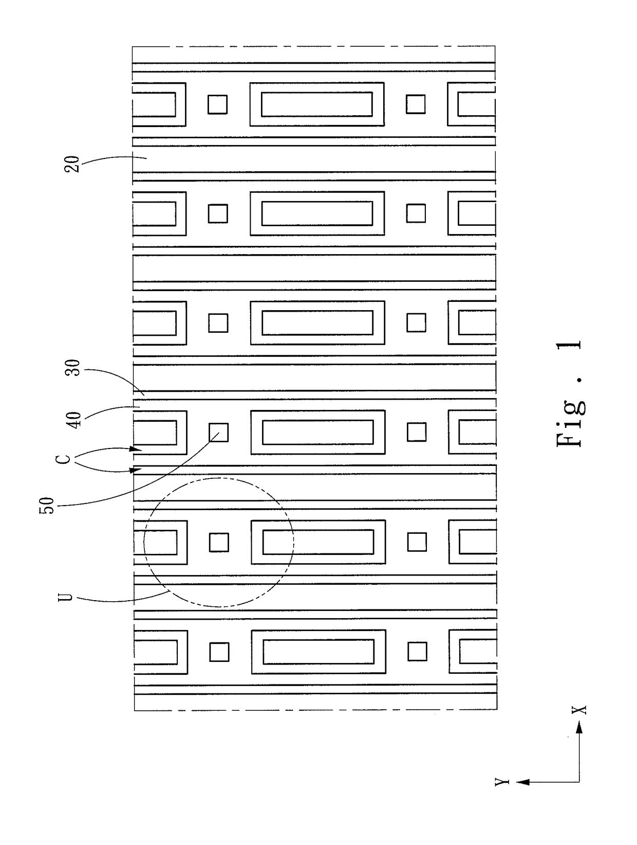
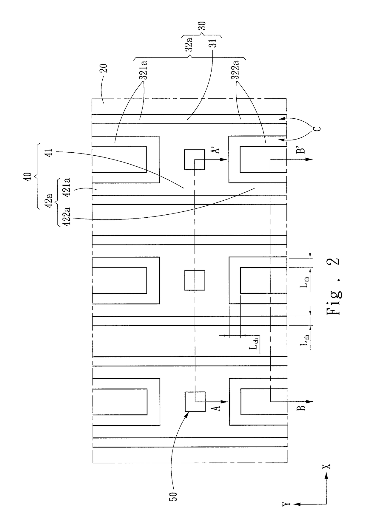
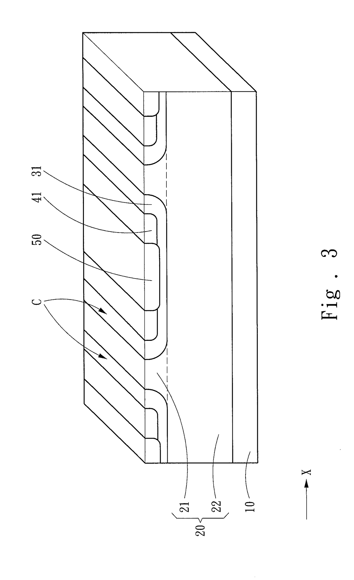

Image

  • Semiconductor power device
  • Semiconductor power device
  • Semiconductor power device

Examples


Embodiment Construction

[0033]The present invention is more thoroughly described with the accompanying drawings below. Embodiments are depicted in these drawings. However, the present invention may be implemented in various forms and the embodiments are not to be construed as limitations to the present invention. The accompanying drawings are illustrative diagrams of ideal embodiments of the present invention. For better clarity, thickness of layers and regions may be enlarged in these drawings. Further, the drawings may not show shape changes resulted from manufacturing processes and / or tolerance. Therefore, the embodiments of the present invention are not to be construed as limiting the specific shapes of the regions in the description, and may include, for example, shape variations caused by manufacturing. For example, a rectangle usually comprises rounded corners in reality.

[0034]In the description, the layers and / or the regions are characterized as having a conductivity type such as n type or p type, ...


PUM


Abstract

A semiconductor power device includes an n-type drift layer, a plurality of first p-doped regions, a plurality of n-doped regions, a plurality of second p-doped regions, a gate dielectric layer, a gate electrode, an interlayer dielectric layer and a plurality of source contacts. Each first p-doped region includes a first p-doped portion and a plurality of first p-doped arms extending outwards from the first p-doped portion. Each n-doped region includes an n-doped portion and a plurality of n-doped arms extending outwards from the n-doped portion.

Description

FIELD OF THE INVENTION[0001]The present invention relates to a semiconductor power device, and particularly to a semiconductor power device having low on-resistance.BACKGROUND OF THE INVENTION[0002]Semiconductor power devices are looking for low on-resistance, and fast switching to reduce conduction loss and switching loss. Common semiconductor power switches include metal-oxide semiconductor field-effect transistors (MOSFET), insulated gate bipolar transistors (IGBT) and junction field-effect transistors (JFET).[0003]Taking MOSFET as an example, the U.S. Pat. No. 7,598,567 discloses a power switching semiconductor device with rectifying junction shunts capable of reducing on-resistance (RDS(on)). The above power switching semiconductor device includes a drift layer, a first body region, a second body region, a contactor region, a shunt channel region, a first terminal and a second terminal. The drift layer comprises a first conductivity type. The first body region is adjacent to th...

Claims


Application Information

Patent Timeline
Patent Type & Authority Applications(United States)
IPC IPC(8): H01L29/06H01L29/10H01L29/16
CPCH01L29/0634H01L29/0696H01L29/1095H01L29/1608H01L29/7395H01L29/7802H01L29/66674
Inventor YEN, CHENG-TYNGHUNG, CHIEN-CHUNGLEE, CHWAN-YING
Owner SHANGHAI HESTIA POWER INC
Learn More