Structures for power transistor and methods of manufacture

a technology of power transistors and structures, applied in the field of structure for a type of power transistor, can solve the problems of high input impedance, small driving power, and rather complex manufacture of this traditional structure, and achieve the effect of reducing gate charge qg, less gate area, and reducing gate area

Inactive Publication Date: 2012-10-04
WUXI VERSINE SEMICON CORP
View PDF2 Cites 0 Cited by
  • Summary
  • Abstract
  • Description
  • Claims
  • Application Information

AI Technical Summary

Benefits of technology

[0015]The beneficial effects of the invention are as follows. The power transistor described by the invention uses a new structure with an isolation structure surrounding two gate units. Compared to the traditional gate structure, the new structure has less gate area. Therefore, the gate charge Qg can be reduced by reducing the gate area. Moreover, the overlap area between the gate and the drain is less and Qgd is reduced effectively. By extra ion implantation onto the drift region, the on-state resistance Rdson can be reduced effectively and improves the FOM further. The manufacture process is simpler. It only needs photo mask when making the gate, etching source region and making source electrode. Because the whole process takes only three (3) masks, the cost is reduced significantly.

Problems solved by technology

Its input impedance is high and driving power is small.
In addition, the manufacture of this traditional structure is rather complex.
Therefore, the production cost is relatively higher.

Method used


Image

  • Structures for power transistor and methods of manufacture
  • Structures for power transistor and methods of manufacture
  • Structures for power transistor and methods of manufacture

Examples


first embodiment

The First Embodiment

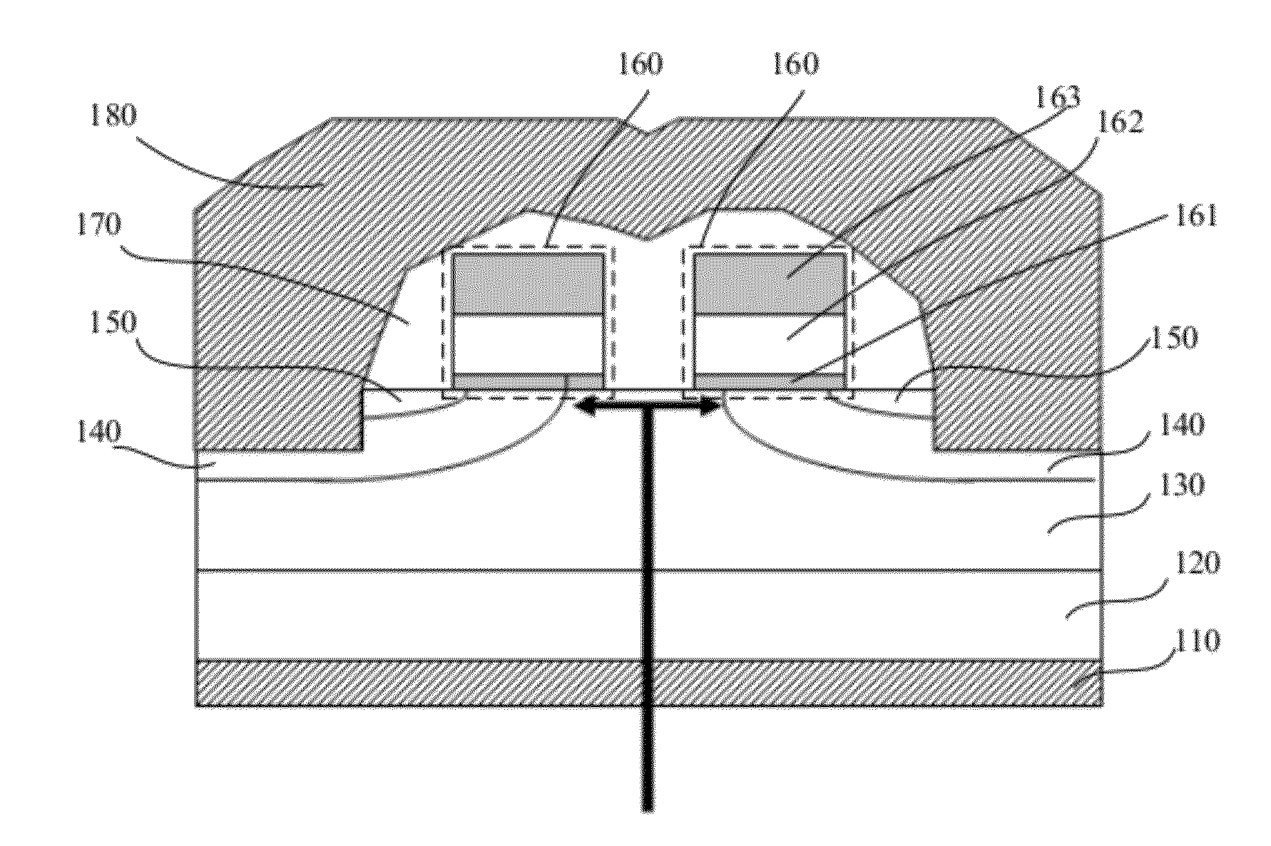
[0021]A MOSFET structure is provided by this embodiment. As shown in FIG. 1, the device structure comprises: a drain electrode 110; a first conductive substrate 120 on the drain electrode 110; a drift region 130 on the first conductive substrate 120; two first conductive source regions 150 located on the two sides of the drift region 130, respectively; two conductive region 140 located between two second conductive regions 140 and the drift region 130; two gate units 160 on the two second conductive region 140, respectively; an isolation structure 170 covers the surface of two gate units 160 and isolates the two gate units 160 electrically; the source electrode 180 covers the surface of the isolation structure 170. The source electrode 180 is connected to two of the first conductive source regions 150 and two of the second conductive body regions 140 electrically.

[0022]In the case of NMOS, the first conductive substrate uses N+ type semiconductor substrate. The d...

second embodiment

The Second Embodiment

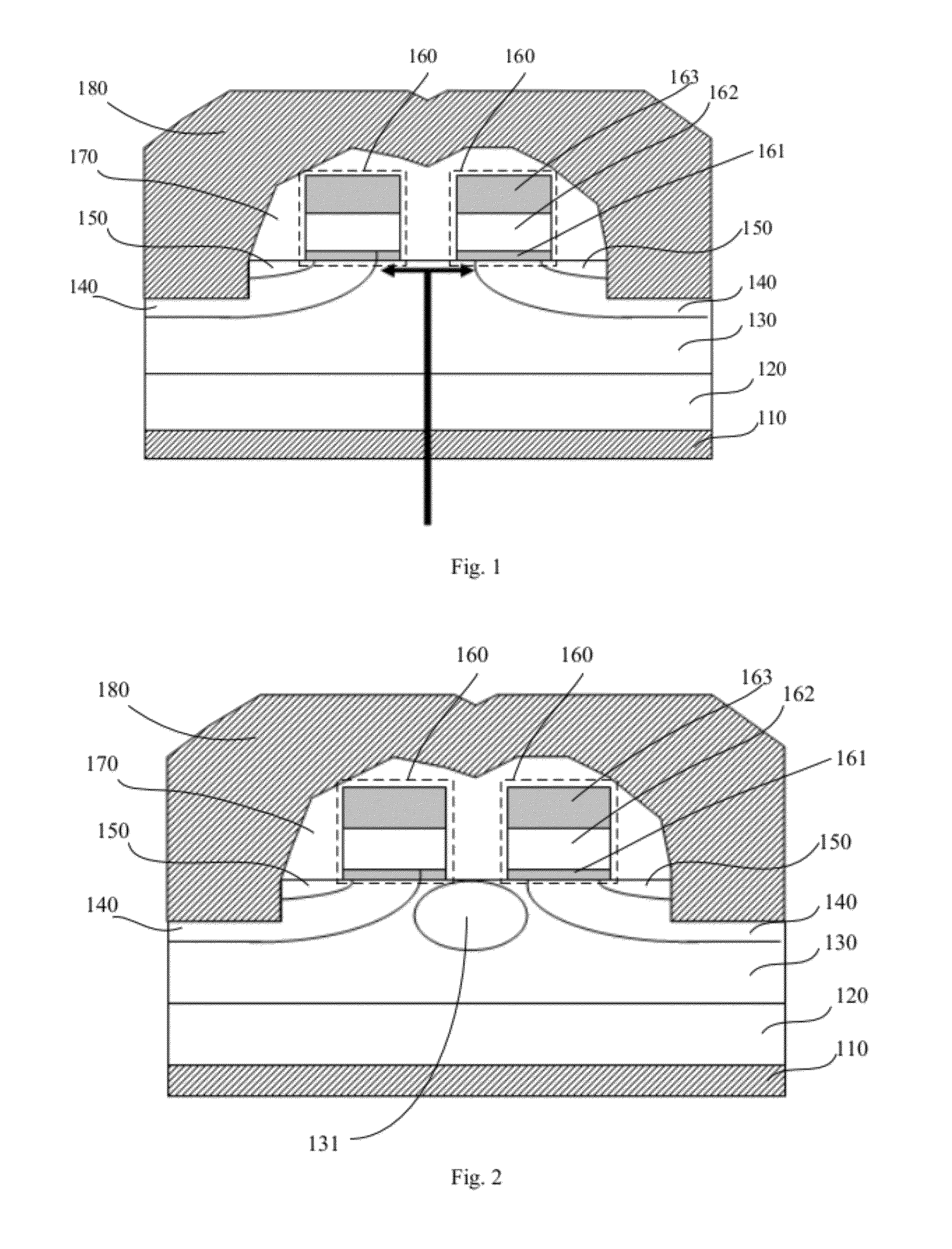
[0035]This embodiment provides a device structure of IGBT, as shown in FIG. 4, which comprises:

[0036]A collector 210, a second conductive substrate region 220 on the collector 210, a drift region 230 on the second conductive substrate 220, two first conductive type emitters on each side of the drift region 230 of the first conductive type, two of the second conductive region 240 located between two of the second conductive emitter 250 and two first conductive drift region 230, two gate units 260 located on two of the second conductive region 240, an isolation structure 270 covering the surface of two gate units 260 and separating two gate units 260 electrically, an emitter 280 covering the surface of the isolation structure 270. The emitter 280 is connected to two of the first conductive emitter 250 and two of the second conductive region 240.

[0037]Wherein, the gate unit 260 comprises a gate dielectric layer 261 and a gate electrode layer 262 on the top of the g...


PUM


Abstract

The invention discloses a manufacture method and structure of a power transistor, which comprises a lower electrode, a substrate, a drift region, two first conductive regions, two second conductive regions, two gate units, an isolation structure and an upper electrode; wherein the two second conductive region are between the two first conductive regions and the drift region; the two gate units are on the two second conductive regions; the isolation structure covers the surface of the two gate units; the upper electrode covers; the surface of the isolation structure and connects to the two first conductive regions and the two second conductive regions electrically. When the substrate is of the first conductive type, the structure can be used as MOSFET. When the substrate is of the second conductive type, the structure can be used as IGBT. This structure has a small gate electrode area, which leads to less Qg, Qgd and Rdson and improves device performance. The manufacture process is simple and the cost is relatively low.

Description

TECHNICAL FIELD[0001]This invention relates to a structure for a type of power transistor and its methods of manufacture, more particularly, to MOSFET (Metal-Oxide-Semiconductor Field-Effect Transistor) and IGBT (Insulated Gate Bipolar Transistor) and its methods of manufacture. It belongs to the field of semiconductor device and manufacture thereof.BACKGROUND OF THE INVENTION[0002]VDMOS and IGBT are two commonly used power transistors. IGBT is comprised of BJT and MOS, which has the advantage of MOSFET's high impedance and BJT's low conduction voltage. It is very suitable for the fields of AC motor, frequency converter, switching power supply, lighting circuit, traction and driving. VDMOS is a voltage controlled device. Under the proper control of the gate voltage, the surface of the semiconductor is inversed and forms a conduction path. Thus, an appropriate amount of current flows vertically between drain and source electrodes. VDMOS has the advantages of both BJT and MOS. Compare...

Claims


Application Information

Patent Timeline
Patent Type & Authority Applications(United States)
IPC IPC(8): H01L29/78H01L21/76
CPCH01L29/0878H01L29/41766H01L29/42376H01L29/1095H01L29/7802H01L29/7396H01L29/0834H01L29/66727
Inventor HUANG, QINBAI, YUMING
Owner WUXI VERSINE SEMICON CORP
Why Eureka
Try Eureka