Flux-guided tunneling magnetoresistive (TMR) sensor for magnetic tape with reduced likelihood of electrical shorting
a technology of magnetic tape and read head, which is applied in the field of read head for magnetic tape, can solve the problems of undesirable overcoat, achieve the effects of shortening the sense current, increasing the spacing, and increasing separation
- Summary
- Abstract
- Description
- Claims
- Application Information
AI Technical Summary
Benefits of technology
Problems solved by technology
Method used
Image

Examples
first embodiment
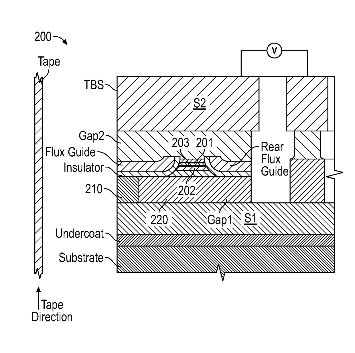
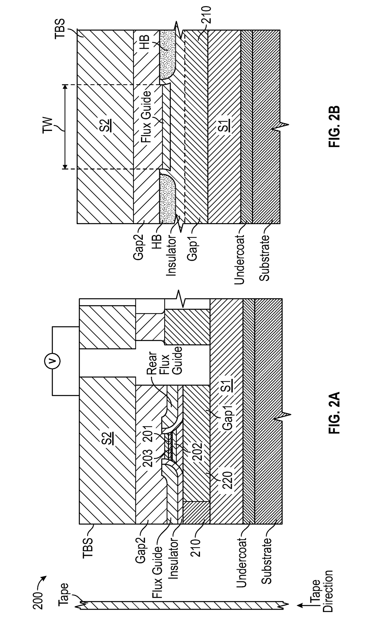
[0021]FIG. 2A is a schematic sectional view of the tape head according to the invention with a TMR sensor and flux guide and shows the tape-bearing surface (TBS) as an edge. FIG. 2B is a view of the tape head of FIG. 2A as viewed from the TBS.
[0022]The tape head 200 is formed on a suitable substrate, such as a composite of aluminum-titanium carbide (AlTiC). A first shield (S1) of soft magnetic material, like a NiFe alloy, is deposited on an undercoat, typically alumina, on the substrate. A first gap layer (gap 1) is made of two portions and is formed on S1. A first portion of gap 1 is non-conducting insulating portion 210 with an edge at the TBS. Portion 210 may be formed of alumina. A second portion of gap 1 is non-magnetic electrically-conducting portion 220 and is located below the TMR sensor. The TMR sensor, which includes free ferromagnetic layer 201, insulating tunnel barrier layer 202, which is typically MgO, and reference ferromagnetic layer 203 is deposited and patterned on...
second embodiment
[0025]FIG. 4A is a schematic sectional view of the tape head according to the invention with a TMR sensor and flux guide and shows the tape-bearing surface (TBS) as an edge. FIG. 4B is a view of the tape head of FIG. 4A as viewed from the TBS. The tape head 300 is like the tape head 200 in FIGS. 2A-2B but includes an insulating isolation layer 330 between gap 1 and shield 1. The isolation layer 330 has an edge at the TBS and may be formed of alumina to a thickness of about 5 to 10 nm. FIG. 4A also shows that the sense circuitry that includes a voltage source has an electrical path for the sense current provided by S2, gap 2, the TMR sensor and conductive portion 220 of gap 1. The sense current does not pass through S1. FIG. 4A also shows an option that S1 and S2 can be connected in a region behind the TMR sensor so that S1 and S2 can be at the same electrical potential.
[0026]An optional protective overcoat, such as a 15 nm film of alumina, may be formed on the TBS in both embodiment...
PUM
| Property | Measurement | Unit |
|---|---|---|
| thickness | aaaaa | aaaaa |
| thickness | aaaaa | aaaaa |
| thickness | aaaaa | aaaaa |
Abstract
Description
Claims
Application Information