Solid-state imaging device and camera

a solid-state imaging and camera technology, applied in the field of solid-state imaging devices and cameras, can solve the problems of increasing row correlation, generating random horizontal line noise, and difficult adjustment, and achieve the effect of suppressing vertical line nois

Active Publication Date: 2017-10-19
PANASONIC SEMICON SOLUTIONS CO LTD
View PDF18 Cites 14 Cited by
  • Summary
  • Abstract
  • Description
  • Claims
  • Application Information

AI Technical Summary

Benefits of technology

[0010]With the solid-state imaging device and the camera according to the present disclosure, it is possible

Problems solved by technology

Such noise and nonuniformities may appear as vertical line noise on an image.
However, because a pixel reset signal is connected commonly to all columns, equivalent noise is superimposed commonly to all columns, which increases row correlation and generates random horizontal line noise.
For this reason, it is necessary to set in advance optimal values by including threshold values of tran

Method used


Image

  • Solid-state imaging device and camera
  • Solid-state imaging device and camera
  • Solid-state imaging device and camera

Examples


embodiment 1

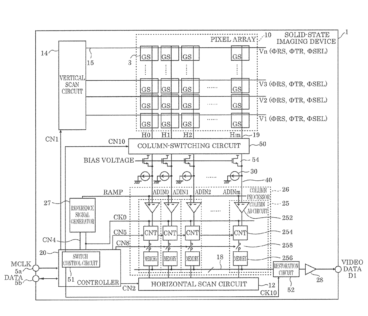
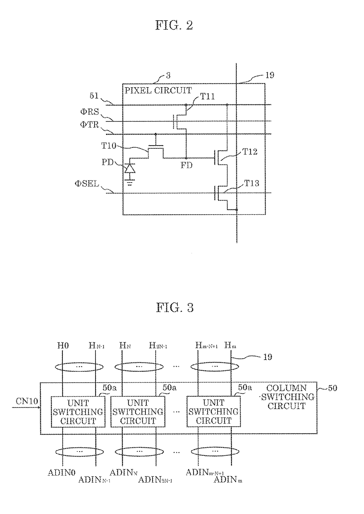
[0036]First, an overview of a solid-state imaging device according to Embodiment 1 will be described. The solid-state imaging device according to the present embodiment is configured to reduce vertical line noise by switching the correspondence relationship between columns of pixel circuits in a pixel array including a plurality of pixel circuits (unit cells or unit pixel cells) that are arranged in rows and columns and columns of column AD circuits provided for each vertical signal line.

[Configuration Example of Solid-State Imaging Device]

[0037]A configuration of the solid-state imaging device according to Embodiment 1 will be described next with reference to the drawings.

[0038]FIG. 1 is a block diagram showing a configuration example of solid-state imaging device 1 according to Embodiment 1. Solid-state imaging device 1 shown in the diagram includes pixel array 10, horizontal scan circuit 12, vertical scan circuit 14, a plurality of vertical signal lines 19, controller 20, column ...

embodiment 2

[0131]In Embodiment 2, in addition to Embodiment 1, a solid-state imaging device that reduces column correlation will be described.

[0132]As described above, the first main factor for the occurrence of vertical line noise is column nonuniformities in the inversion speeds of voltage comparators 252, and the second main factor is column nonuniformities in the response speeds of vertical signal lines 19.

[0133]Further reduction of vertical line noise caused by column nonuniformities in the inversion speeds of voltage comparators 252 that is the first main factor will be described. In the solid-state imaging device according to the present embodiment, each voltage comparator 252 includes a comparator current source having switchable current characteristics. With this configuration, the column nonuniformities in the inversion speeds of voltage comparators 252 can be reduced.

[0134]Further reduction of vertical line noise caused by column nonuniformities in the response speeds of vertical si...

embodiment 3

[0172]In Embodiment 3, a solid-state imaging device that improves column nonuniformities in the inversion speeds of voltage comparators 252 that is the first main factor will be described in comparison with Embodiment 1.

[0173]Hereinafter, a configuration of a solid-state imaging device according to Embodiment 3 will be described with reference to the drawings.

[0174]FIG. 14 is a block diagram showing a configuration example of solid-state imaging device 1 according to Embodiment 3. Solid-state imaging device 1 shown in the diagram is different from that shown in FIG. 1 in that the position of connection of load current sources 30 to vertical signal lines 19 is upstream of column-switching circuit 50, and clip transistors 54 have been removed. The following description will be given focusing on the differences.

[0175]Load current sources 30 are provided for each column and are connected to vertical signal lines 19 between pixel array 10 and column-switching circuit 50.

[0176]Also, clip ...


PUM


Abstract

A solid-state imaging device includes: a pixel array including a plurality of pixel circuits arranged in rows and columns; a vertical signal line that is provided for each of the columns and transmits pixel signals; a column AD circuit that is provided for each of the columns and AD converts the pixel signals from the vertical signal line; a column-switching circuit that is interposed in the vertical signal line between the pixel array and the column AD circuit and switches connection between the vertical signal line and the column AD circuit; a controller that causes the column-switching circuit to switch the connection for every horizontal scan period; and a restoration circuit that restores ordering of the AD converted signals so as to correspond to ordering in which the vertical signal lines are arranged in the pixel array.

Description

CROSS REFERENCE TO RELATED APPLICATIONS[0001]This application is a U.S. continuation application of PCT International Patent Application Number PCT / JP2016 / 000317 filed on Jan. 22, 2016, claiming the benefit of priority of Japanese Patent Application Number 2015-014822 filed on Jan. 28, 2015, the entire contents of which are hereby incorporated by reference.BACKGROUND1. Technical Field[0002]The present disclosure relates to a solid-state imaging device, and a camera.2. Description of the Related Art[0003]In a column-parallel output-type solid-state imaging device, signals of the same column are analog-to-digital (AD) converted by the same processing circuit provided for each column. Nonuniformities in the processing circuits each provided for each column and column noise inherently have column correlation. Such noise and nonuniformities may appear as vertical line noise on an image.[0004]Japanese Unexamined Patent Application Publication No. 2008-60872 (hereinafter, referred to as PT...

Claims


Application Information

Patent Timeline
IPC IPC(8): H04N5/365H04N5/378H04N5/374
CPCH04N5/365H04N5/378H04N5/374H04N25/677H04N25/75H04N25/67H04N25/76
Inventor IKUMA, MAKOTOTSUNODA, MANABUWATANABE, KENJIHAGA, KENICHIKATO, MASARU
Owner PANASONIC SEMICON SOLUTIONS CO LTD
Why Eureka
Try Eureka