3-dimensional non-volatile memory device and method of fabricating the same

a non-volatile memory and 3d technology, applied in the field of semiconductor technology, can solve the problems of increasing the complexity of the fabrication process, and increasing the cost of data storag

Active Publication Date: 2017-11-23
IND ACADEMIC CORP FOUND YONSEI UNIV
View PDF13 Cites 23 Cited by
  • Summary
  • Abstract
  • Description
  • Claims
  • Application Information

AI Technical Summary

Benefits of technology

[0006]Provided is a 3-dimensional non-volatile memory device capable of increasing data storage capacity based on a simple design modification.

Problems solved by technology

Recently, downscaling the NAND flash memory device with a conventional two-dimensional (2D) memory cell array architecture has become more difficult as 20 nm or smaller photolithography techniques have reached their limits.
In addition, design issues, which are related to reduction of a sensing margin in accordance with reduction of a number of electrons stored in a data storage film (e.g., a floating gate), and related to disturbances between memory cells, have become barriers against the downscaling of the conventional 2D memory cell array architecture.
Conventionally, there is an approach to increase the number of gate layers in a conventional structure or to form a single memory cell as a multi-bit memory cell, but the fabricating process therefor becomes more complicated.

Method used


Image

  • 3-dimensional non-volatile memory device and method of fabricating the same
  • 3-dimensional non-volatile memory device and method of fabricating the same
  • 3-dimensional non-volatile memory device and method of fabricating the same

Examples


Embodiment Construction

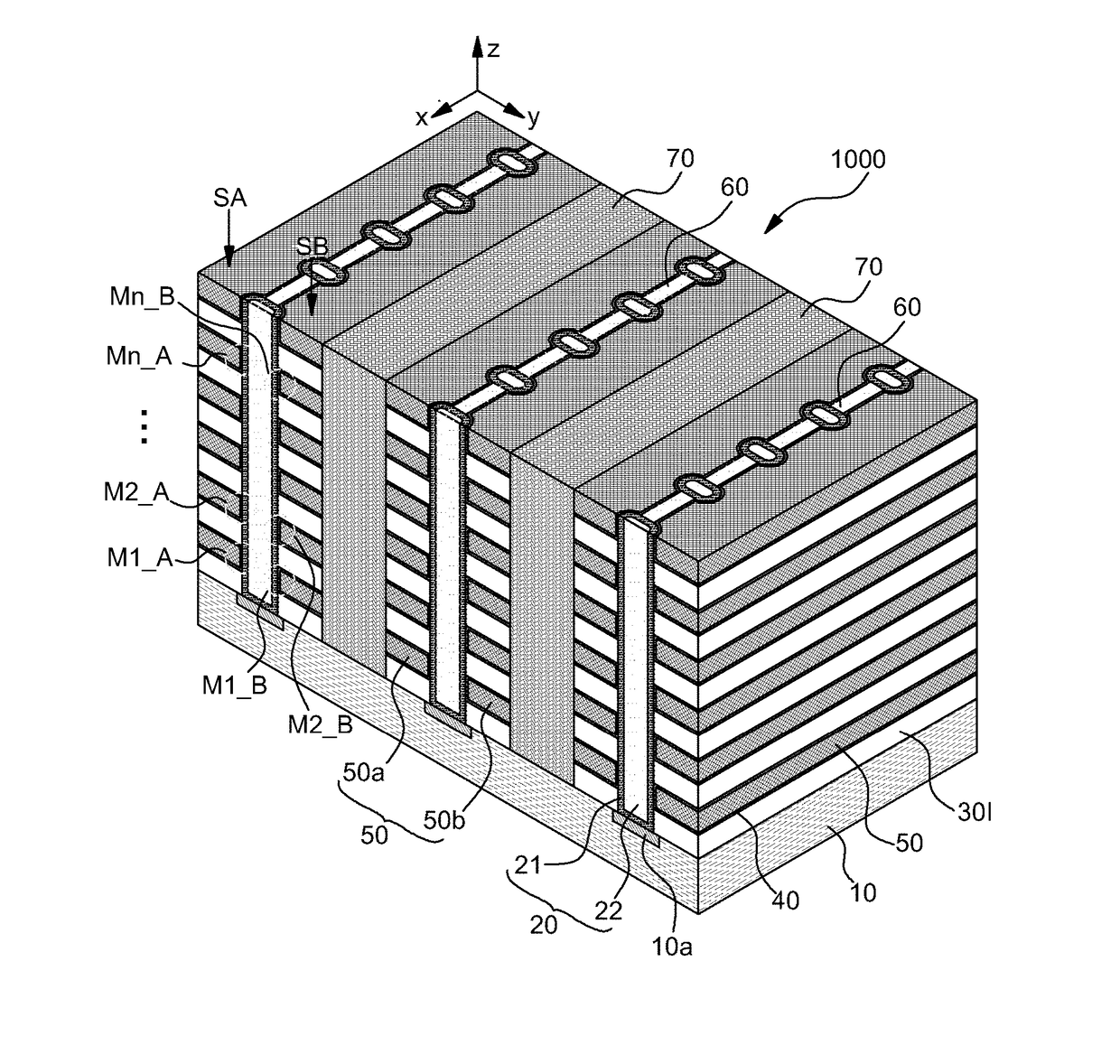
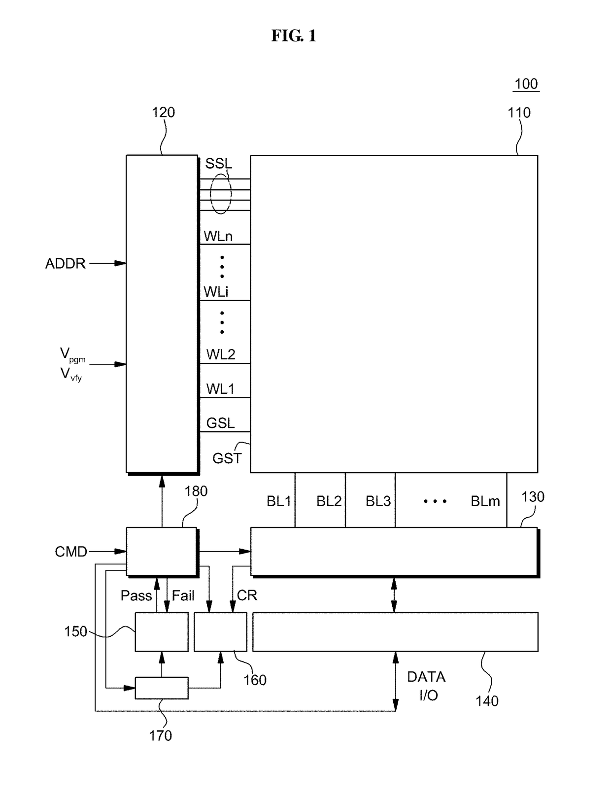
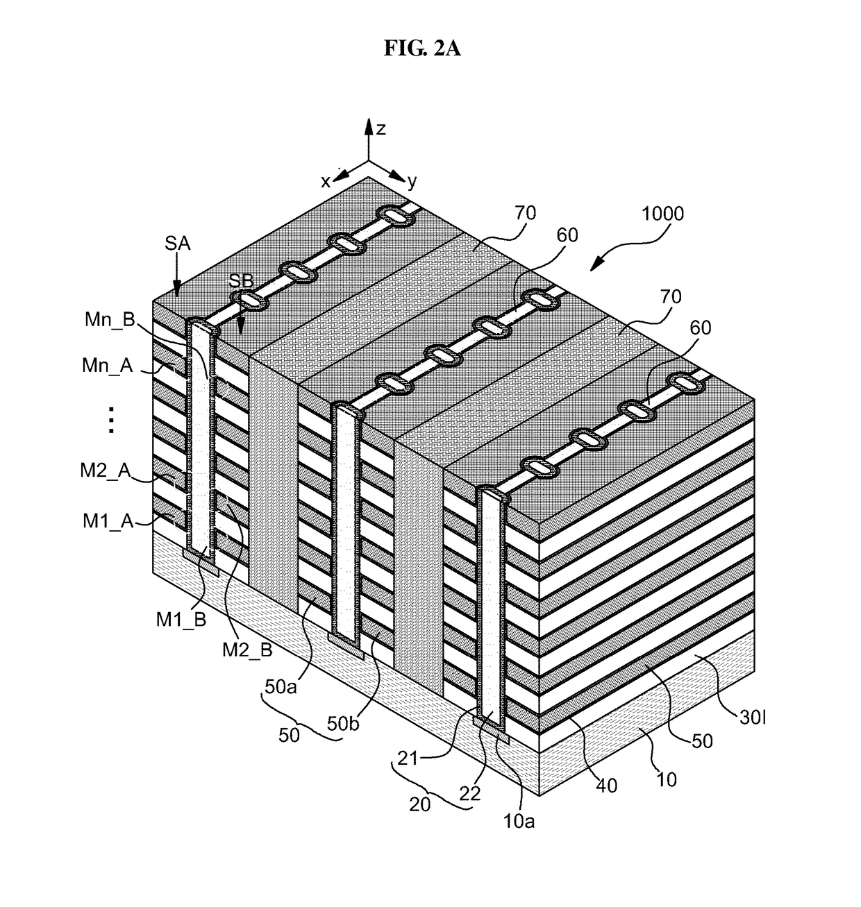
[0030]The present invention now will be described more fully hereinafter with reference to the accompanying drawings, in which embodiments of the invention are shown. This invention may, however, be embodied in many different forms and should not be construed as limited to the embodiments set forth herein. Rather, these embodiments are provided so that this disclosure will be thorough and complete, and will fully convey the scope of the invention to those skilled in the art.

[0031]The terminology used herein is for the purpose of describing particular embodiments only and is not intended to be limiting of the invention. As used herein, the singular forms “a”, “an” and “the” are intended to include the plural forms as well, unless the context clearly indicates otherwise. It will be further understood that the terms “includes”, “comprises” and / or “comprising,” when used in this specification, specify the presence of stated features, integers, steps, operations, elements, and / or compone...


PUM


Abstract

Provided are a 3-dimensional non-volatile memory device and a method of fabricating the same. The 3-dimensional non-volatile memory device may include a substrate; semiconductor pillars, which are arranged at a certain interval in a first direction and a second direction different from the first direction; a string isolation film, which is arranged between the semiconductor pillars arranged in the first direction among the semiconductor pillars and extends in the first direction and a third direction vertical to the main surface of the substrate; first sub-electrodes repeatedly stacked on the substrate in the third direction; second sub-electrodes, which are electrically isolated from the first sub-electrodes by the string isolation film, and are repeatedly stacked on the substrate in the third direction; and information storage films including a first information storage film and a second information storage film.

Description

CROSS-REFERENCE TO RELATED APPLICATION[0001]This application claims priority of Korean Patent Application No. 10-2016-0061462, filed on May 19, 2016, in the KIPO (Korean Intellectual Property Office), the disclosure of which is incorporated herein entirely by reference.BACKGROUND OF THE INVENTIONField of the Invention[0002]The present disclosure relates to a semiconductor technique, and more particularly, to a 3-dimensional non-volatile memory device and a method of fabricating the same.Description of the Related Art[0003]Due to increasing demands for portable application devices, such as digital cameras, smart phones, and tablet PCs, and replacement of conventional hard disk drives with solid-state drives (SSDs), markets for non-volatile memory devices are rapidly growing. Among the non-volatile memory devices, NAND flash memory devices are popular due to low manufacturing cost for high degree of integration.[0004]Recently, downscaling the NAND flash memory device with a convention...

Claims


Application Information

Patent Timeline
Patent Type & Authority Applications(United States)
IPC IPC(8): H01L27/11582H01L27/11524H01L27/11556H01L27/1157
CPCH01L27/11582H01L27/11556H01L27/11524H01L27/1157H01L29/40117H10B43/27H10B41/35H10B41/20H10B41/27H10B43/30H10B43/35H10B43/20H10B41/30
Inventor SOHN, HYUN CHULNA, HEE DOKIM, YOUNG MO
Owner IND ACADEMIC CORP FOUND YONSEI UNIV
Why Eureka
Try Eureka