
Electro-optical device stack

a technology of optical devices and stacks, applied in optical elements, organic semiconductor devices, instruments, etc., can solve the problems of reducing specular transmittance, reducing the efficiency of reducing the efficiency of achieving 100 lm/w or higher, so as to achieve less haziness, less visible, and improve the effect of scattering efficiency

Inactive Publication Date: 2018-01-11
NEDERLANDSE ORG VOOR TOEGEPAST-NATUURWETENSCHAPPELIJK ONDERZOEK (TNO)
View PDF4 Cites 3 Cited by
  • Summary
  • Abstract
  • Description
  • Claims
  • Application Information

AI Technical Summary

Benefits of technology

The patent describes an optical scattering layer that can improve the out-coupling of light in devices such as OLEDs. The layer uses scattering particles that match the refractive index of the material in which they are embedded. This results in high scattering efficiency and minimal haziness when viewing the layer from different angles. The layer can also be used in micro-cavity devices to improve the scattering efficiency and provide a barrier layer for moisture and oxygen. The refractive indices of the particles and the matrix material can be chosen to optimize the scattering ratio and minimize the impact of polarization. Overall, the optical scattering layer can enhance the out-coupling of light and improve the performance of optical devices.

Problems solved by technology

Without such layer, reaching an efficiency of 100 lm / W or higher is difficult.
However, the scattering layer may result in haziness.
For example, when a transparent device is provided, it can be disadvantageous that a specular transmittance is reduced by adding the scattering layer.
For example, when a reflecting back surface is provided, it can be disadvantageous that a mirror-like appearance of the device is lost by adding the scattering layer.

Method used


Image

  • Electro-optical device stack
  • Electro-optical device stack
  • Electro-optical device stack

Examples


Embodiment Construction

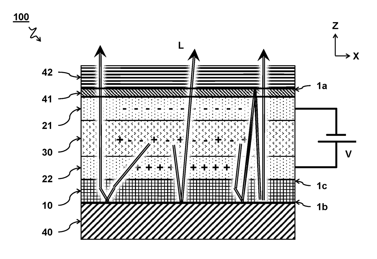
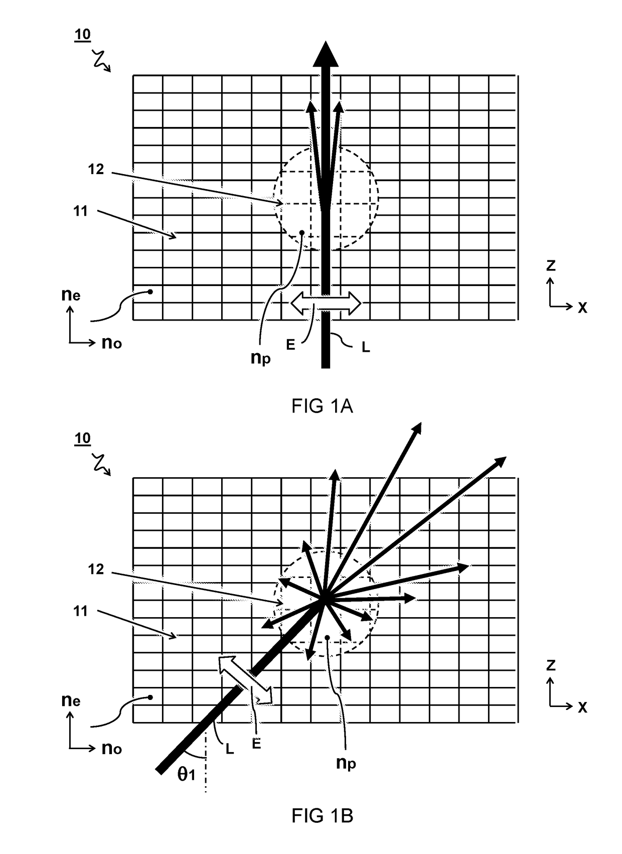
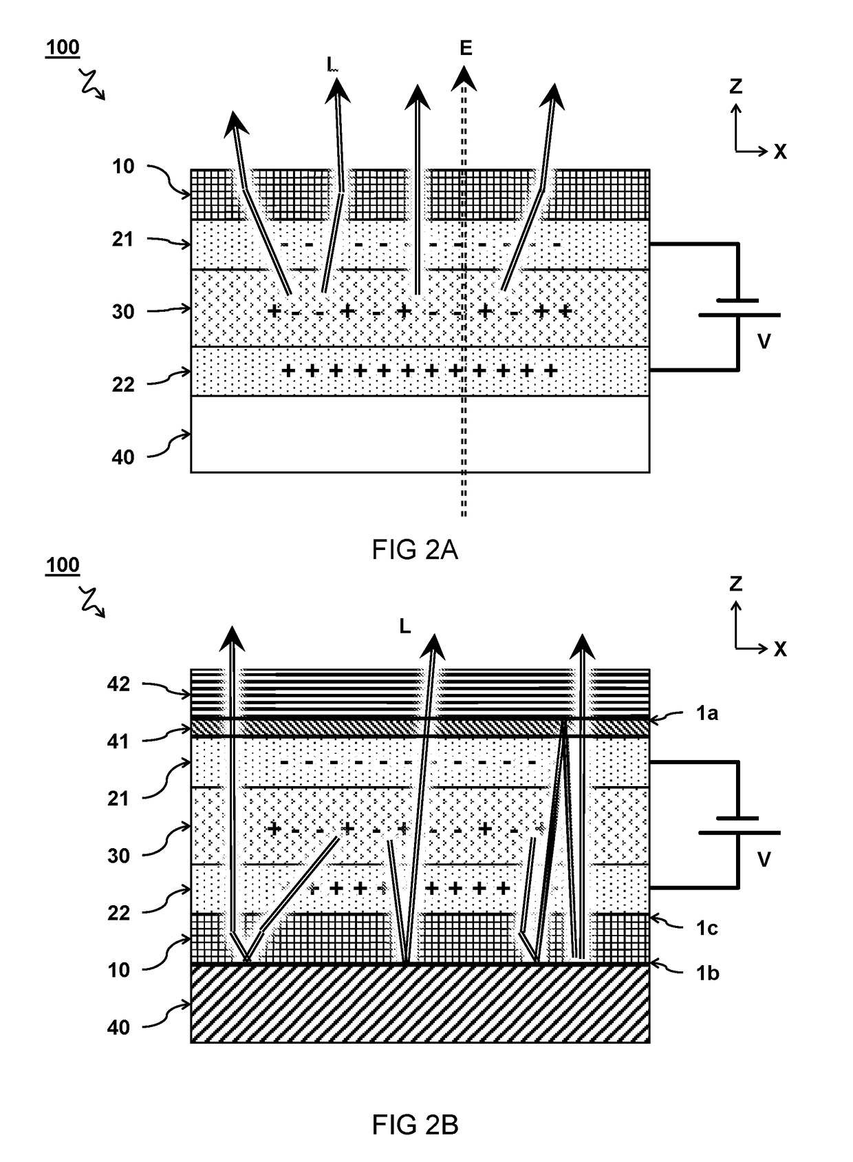
[0019]Unless otherwise defined, all terms (including technical and scientific terms) used herein have the same meaning as commonly understood by one of ordinary skill in the art to which this invention belongs as read in the context of the description and drawings. It will be further understood that terms, such as those defined in commonly used dictionaries, should be interpreted as having a meaning that is consistent with their meaning in the context of the relevant art and will not be interpreted in an idealized or overly formal sense unless expressly so defined herein. In some instances, detailed descriptions of well-known devices and methods may be omitted so as not to obscure the description of the present systems and methods. Terminology used for describing particular embodiments is not intended to be limiting of the invention. As used herein, the singular forms “a”, “an” and “the” are intended to include the plural forms as well, unless the context clearly indicates otherwise...


PUM


Abstract

An optical scattering layer (10) comprising a birefringent matrix material (11) and a plurality of scattering particles (12) dispersed in the matrix material (11). The scattering particles (12) have a particle refractive index (“np”) that for visible light matches the ordinary refractive index (“no”). By matching the refractive index of the scattering particles with one of the refractive indices of the birefringent matrix material, anisotropic scattering is obtained.

Description

TECHNICAL FIELD AND BACKGROUND[0001]The present disclosure relates to an electro-optical device stack comprising an optical scattering layer, an electronic device comprising the electro-optical device stack, and a method for manufacturing the optical scattering layer.[0002]An optical scattering layer may alter (scatter) a direction of light traveling though the layer. This can improve out-coupling e.g. in an electro-optical device stack wherein light is redirected to outside the device. For example, out-coupling by means of a scattering layer can be advantageous to raise the efficiency of an electro-optical device such as an OLED. Without such layer, reaching an efficiency of 100 lm / W or higher is difficult. However, the scattering layer may result in haziness. For example, when a transparent device is provided, it can be disadvantageous that a specular transmittance is reduced by adding the scattering layer. For example, when a reflecting back surface is provided, it can be disadva...

Claims


Application Information

Patent Timeline
Patent Type & Authority Applications(United States)
IPC IPC(8): H01L51/52H01L51/56
CPCH01L51/5268H01L51/5271H01L51/5253H01L51/5275H01L51/56H01L2251/5369G02B5/0242G02B5/3083G02B5/3008H10K59/878H10K59/877H10K59/879H10K2102/331H10K50/854H10K50/844H10K50/856H10K50/858H10K71/00
Inventor HARKEMA, STEPHAN
Owner NEDERLANDSE ORG VOOR TOEGEPAST-NATUURWETENSCHAPPELIJK ONDERZOEK (TNO)
Learn More