

Method of achieving low write latency in a data storage system
a data storage system and write latency technology, applied in the field of data storage systems, can solve the problem that the command management of the conventional pcie nvme based ssds cannot guarantee a deterministic latency of the application, and achieve the effect of low write latency
- Summary
- Abstract
- Description
- Claims
- Application Information
AI Technical Summary
Benefits of technology
Problems solved by technology
Method used
Image

Examples
Embodiment Construction
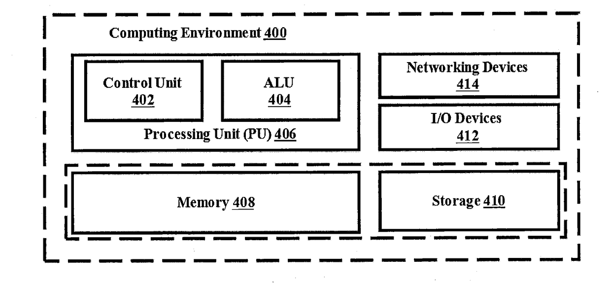
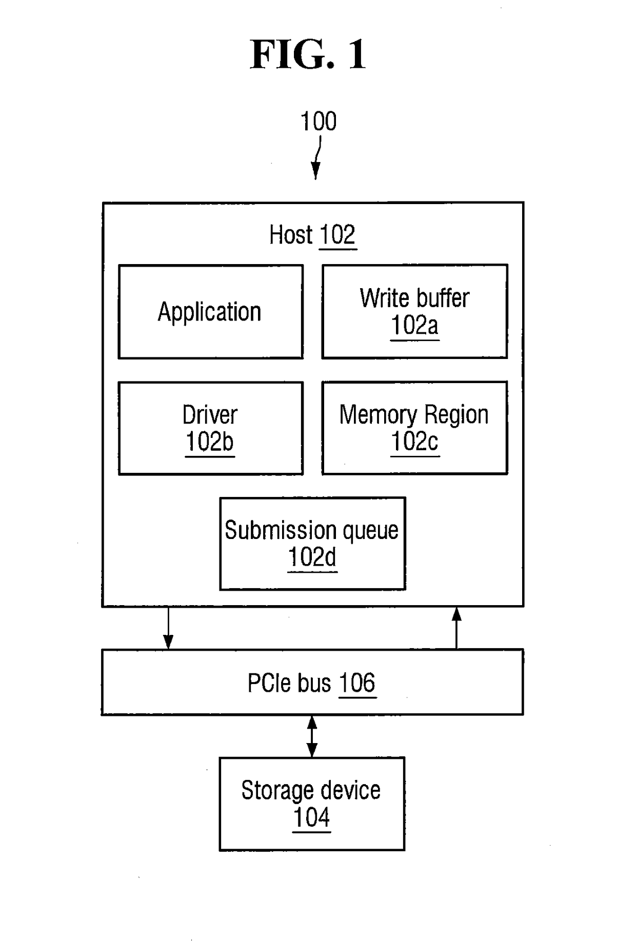
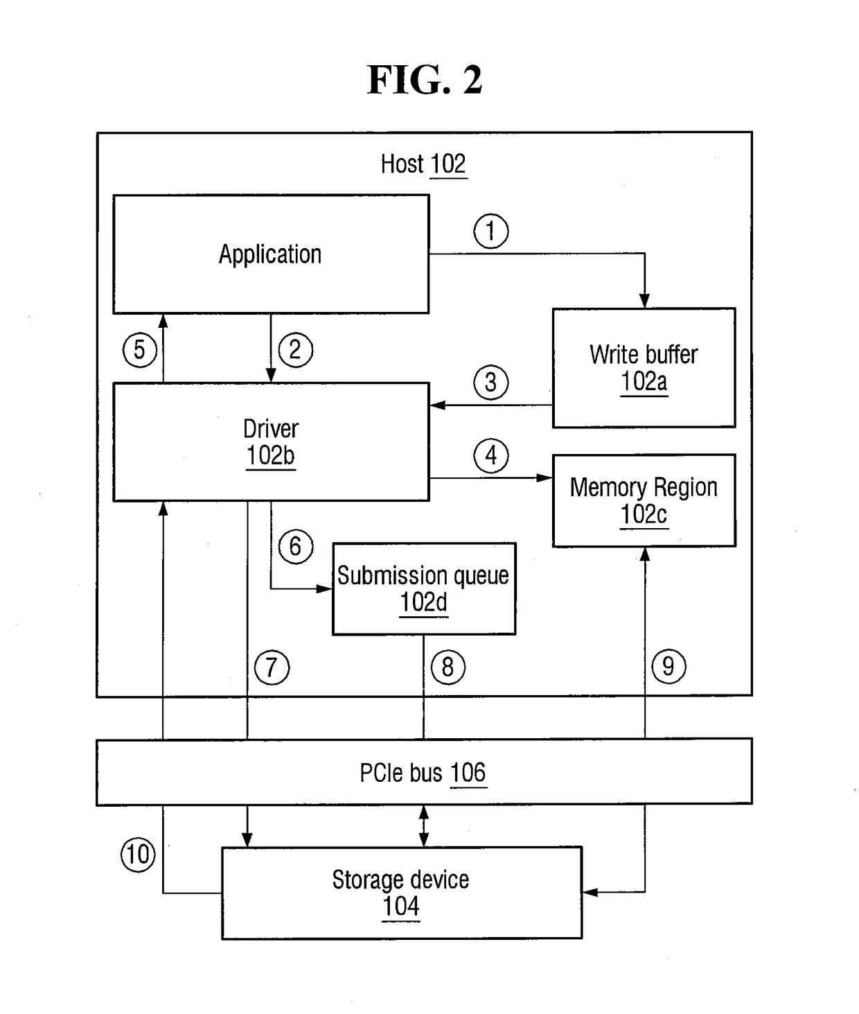
[0021]The embodiments herein and the various features and advantageous details thereof are explained more fully with reference to the non-limiting embodiments that are illustrated in the accompanying drawings and detailed in the following description. Descriptions of well-known components and processing techniques are omitted so as to not unnecessarily obscure the embodiments herein. Also, the various embodiments described herein are not necessarily mutually exclusive, as some embodiments can be combined with one or more other embodiments to form new embodiments. The term “or” as used herein, refers to a non-exclusive or, unless otherwise indicated. The examples used herein are intended merely to facilitate an understanding of ways in which the embodiments herein can be practiced and to further enable those skilled in the art to practice the embodiments herein. Accordingly, the examples should not be construed as limiting the scope of the embodiments herein.
[0022]The embodiments her...
PUM
 Abstract
Description
Claims
Application Information