Semiconductor device and manufacturing method thereof

a technology of semiconductor devices and manufacturing methods, applied in the direction of semiconductor devices, basic electric elements, electrical appliances, etc., can solve the problems of limiting the degree of integration improvement, and the 3d vnand device may not be normally operated, so as to prevent the reduction of charge and the imbalance of charge distribution

Active Publication Date: 2018-02-15
ASM IP HLDG BV
View PDF4 Cites 326 Cited by
  • Summary
  • Abstract
  • Description
  • Claims
  • Application Information

AI Technical Summary

Benefits of technology

[0006]The present invention has been made in an effort to provide a semiconductor device and a manufacturing method thereof that may prevent a reduction of charge from being able to occur in a channel layer of a 3-dimentional vertical NAND flash memory.
[0024]According to the embodiments of the present invention, it is possible to prevent a reduction of charge and imbalance of charge distribution from occuring in a channel layer with a 3-dimentional vertical structure.

Problems solved by technology

Recently, although a flash memory semiconductor has been highly integrated, there is a limit in improvement of the degree of integration due to a physical limit such as an increase of current leakage in a channel according to a conventional 2-dimentional gate structure.
However, since charge distribution is non-uniform in the vertically stacked polysilicon channel layer of the 3D VNAND device, the 3D VNAND device may not be normally operated.

Method used


Image

  • Semiconductor device and manufacturing method thereof
  • Semiconductor device and manufacturing method thereof
  • Semiconductor device and manufacturing method thereof

Examples


Embodiment Construction

[0028]The present invention will be described more fully hereinafter with reference to the accompanying drawings, in which exemplary embodiments of the invention are shown. As those skilled in the art would realize, the described embodiments may be modified in various different ways, all without departing from the spirit or scope of the present invention.

[0029]In the drawings, the thickness of layers, films, panels, regions, etc., are exaggerated for clarity. Like reference numerals designate like elements throughout the specification. It will be understood that when an element such as a layer, film, region, or substrate is referred to as being “on” another element, it can be directly on the other element or intervening elements may also be present. In contrast, when an element is referred to as being “directly on” another element, there are no intervening elements present.

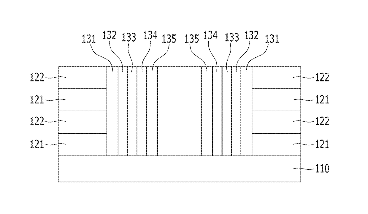
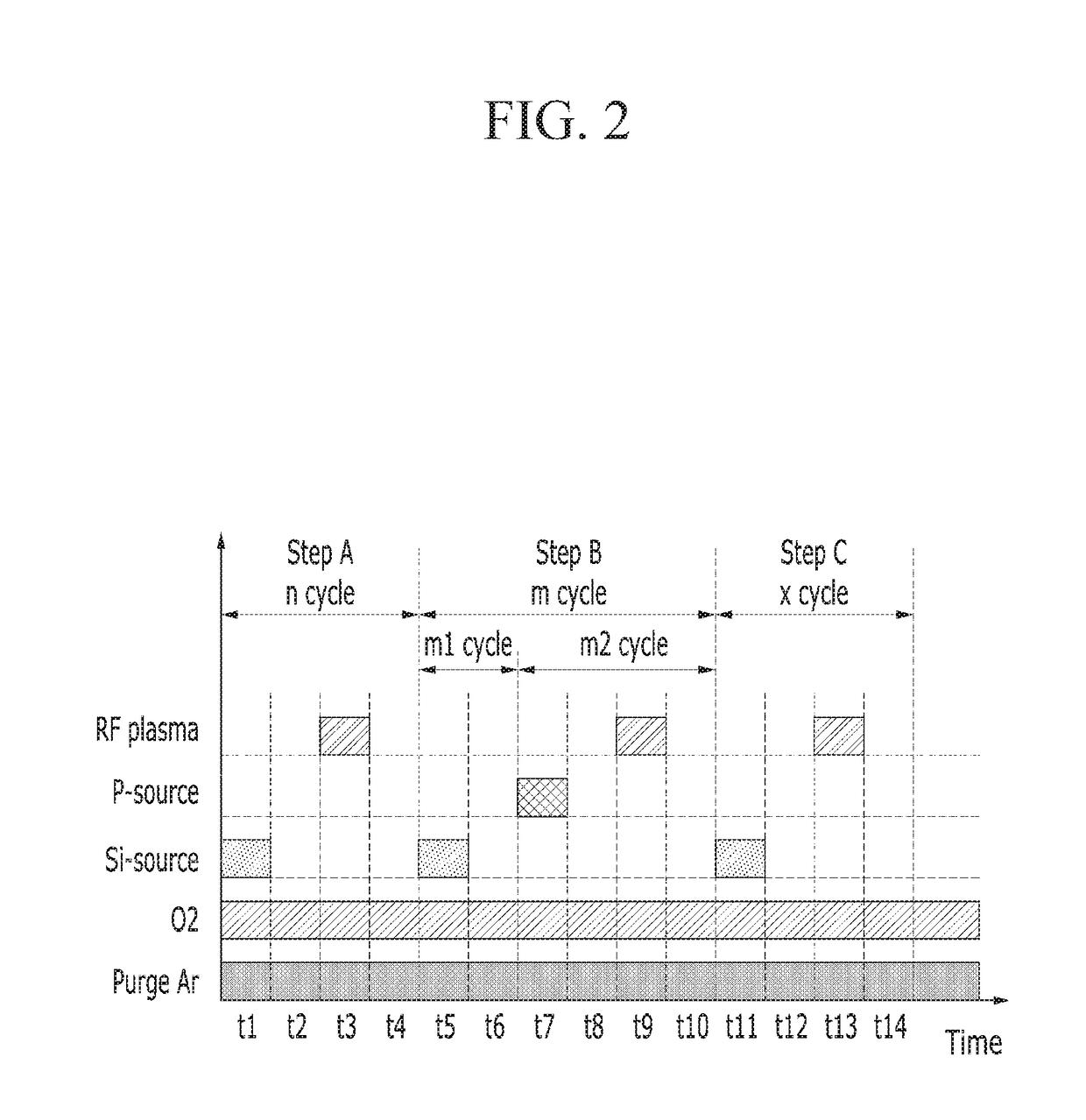
[0030]First, a semiconductor device according to an exemplary embodiment of the present invention will be descr...


PUM


Abstract

Disclosed are a semiconductor device and a manufacturing method thereof. According to the semiconductor device and the manufacturing method thereof according to exemplary embodiments of the present invention, after the dopant source layer is uniformly deposited on a channel layer of the device with the 3-demensional vertical structure by the plasma-enhanced atomic layer deposition (PEALD) method, the deposited dopant source layer is heat-treated so that the dopants are diffused into the channel layer to function as charge carriers, thereby preventing the charges in the channel layer from being reduced. According to the exemplary embodiments of the present invention, the diffusion speed and concentration of the dopant may be controlled by forming the barrier layer between the channel layer and the dopant source layer.

Description

CROSS-REFERENCE TO RELATED APPLICATION[0001]This application is a continuation of U.S. patent application Ser. No. 14 / 938,180 filed Nov. 11, 2015, which claims priority to and the benefit of Korean Patent Application No. 10-2014-0186115 filed in the Korean Intellectual Property Office on Dec. 22, 2014, the entire contents of which are incorporated herein by reference.BACKGROUND OF THE INVENTION(a) Field of the Invention[0002]The present invention relates to a semiconductor device and a manufacturing method thereof.(b) Description of the Related Art[0003]Recently, although a flash memory semiconductor has been highly integrated, there is a limit in improvement of the degree of integration due to a physical limit such as an increase of current leakage in a channel according to a conventional 2-dimentional gate structure.[0004]Thus, a novel structure that is able to substitute for the conventional 2-dimentional gate structure, for example, a 3-dimentional vertical NAND (3D VNAND) flash...

Claims


Application Information

Patent Timeline
Patent Type & Authority Applications(United States)
IPC IPC(8): H01L21/225H01L21/28
CPCH01L21/2255H01L27/11582H01L21/28282H01L29/40117H10B43/27H10B41/30
Inventor KIM, YOUNG JAECHOI, SEUNG WOOYOO, YONG MIN
Owner ASM IP HLDG BV
Why Eureka
Try Eureka