Organic Light Emitting Display Device and Driving Method Thereof

a technology of light-emitting display device and driving method, which is applied in the direction of instruments, static indicating devices, etc., can solve the problem of not being able to detect a small substance insid

Active Publication Date: 2018-03-01
LG DISPLAY CO LTD
View PDF2 Cites 20 Cited by
  • Summary
  • Abstract
  • Description
  • Claims
  • Application Information

AI Technical Summary

Benefits of technology

[0008]In one general aspect, the present disclosure provides an organic light emitting display device including a display panel, a data driver, and a scan driver. The display panel includes sub-pixels. The data driver supplies a data pixel to the sub-pixels. The scan driver supplies a scan signal for controlling a switching transistor of each sub-pixel, and a sensing signal for controlling a sensing transistor of each sub-pixel. The sensing transistor has a turn-on time for detecting whether a short has occurred between at least two electrodes of a switching transistor in response to a sensing signal.
[0009]In another general aspect, the present disclosure provides a driving method of an organic light emitting display device including an initialization step, a program step, a charging step, and a sensing step. The initialization step inclu

Problems solved by technology

However, in the inspection process, it is impossible to detect a small substance, which has come inside during the proces

Method used


Image

  • Organic Light Emitting Display Device and Driving Method Thereof
  • Organic Light Emitting Display Device and Driving Method Thereof
  • Organic Light Emitting Display Device and Driving Method Thereof

Examples


experimental example

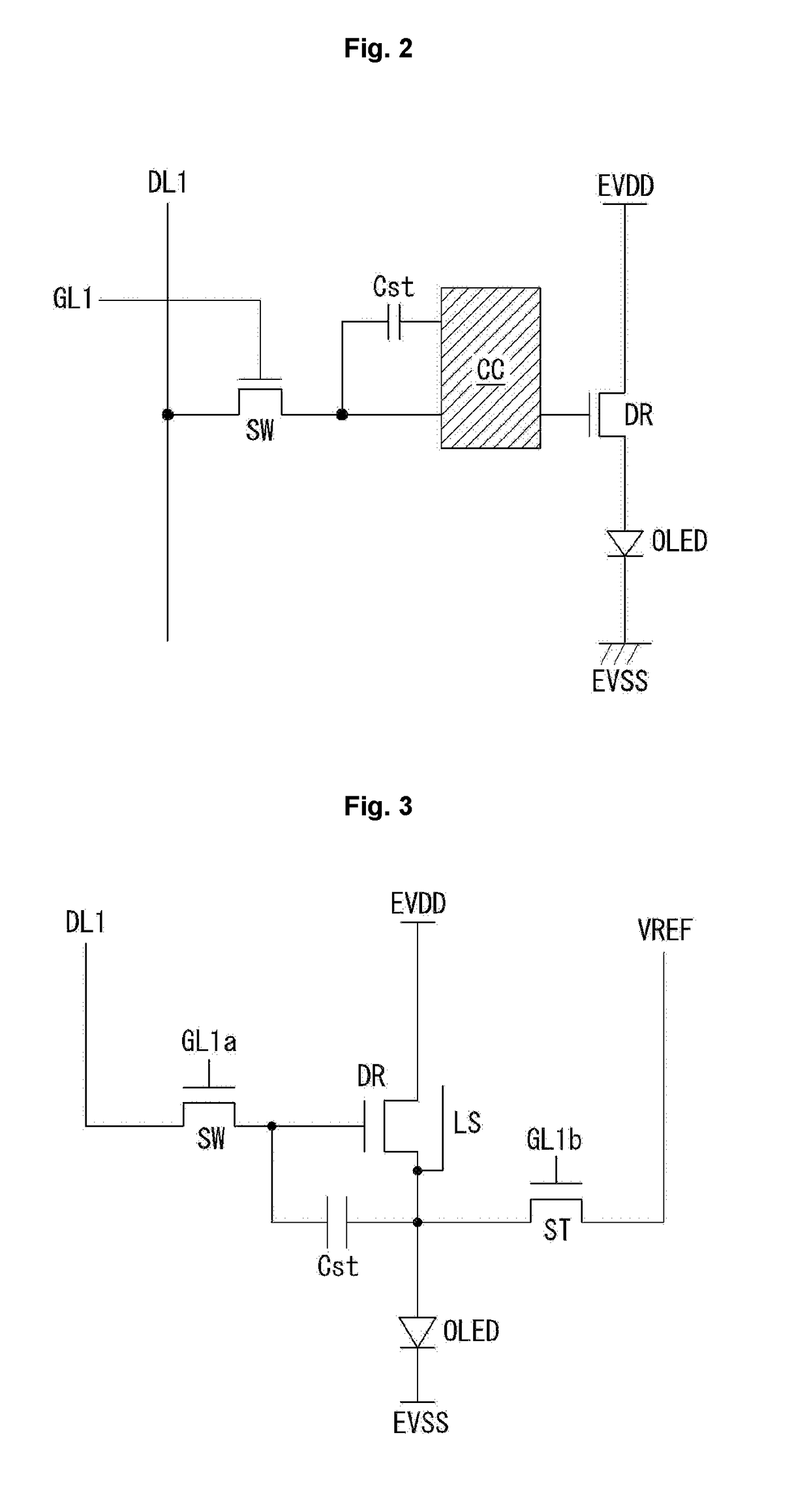
[0085]FIG. 9 is an example of a sub-pixel according to an experimental example, and FIG. 10 is a diagram for explanation of a problem caused by a growing defect.

[0086]FIG. 9 shows a case in which a short between the gate electrode and the second electrode of the switching transistor SW occurs due to a growing defect. The gate electrode of the switching transistor SW is connected to the first scan line A GL1a, and the second electrode of the switching transistor SW is connected to the gate electrode of the driving transistor DR.

[0087]A scan signal provided via the first scan line A GL1a temporarily becomes logic high in a period of one frame in order to transfer a data signal to a sub-pixel SP, and then maintained at logic low until the next frame comes.

[0088]Meanwhile, when a short occurs between the gate electrode and the second electrode of the switching transistor SW, not just the gate electrode of the driving transistor DR but the second electrode thereof is affected. As a resul...

embodiment

[0095]FIG. 11 is a waveform for explanation of a short detection method according to an embodiment. FIGS. 12 to 15 are diagrams for explanation of each step of a short detection operation, shown in FIG. 11. FIG. 16 is a diagram illustrating a sensing voltage according to a state of a switching transistor. FIG. 17 is a flowchart for explanation of a compensation method depending on presence or absence of a short, according to an embodiment.

[0096]As illustrated in FIG. 11, a short detection method according to an embodiment includes an initialization period 1, a program period 2, a charging period 3, and a sensing period 4.

[0097]A scan signal SCAN is maintained at logic high in the program period 2, while being maintained at logic low in the initialization period 1, the charging period 3, and the sensing period 4. A sensing signal SENS is maintained at logic low in the program period 2, while being maintained at logic high in the initialization period 1, the charging period 3, and the...


PUM


Abstract

An organic light emitting display device includes a display panel, a data driver, and a scan driver. The display panel includes sub-pixels. The data driver supplies a data signal to the sub-pixels. The scan driver supplies a scan signal for controlling a switching transistor of each sub-pixel, and a sensing signal for controlling a sensing transistor of each sub-pixel. The sensing transistor has a turn-on time for detecting whether a short has occurred between at least two electrodes of a switching transistor in response to a sensing signal.

Description

[0001]This application claims priority to Republic of Korea Patent Application No. 10-2016-0111803, filed on Aug. 31, 2016, which is incorporated herein by reference for all purposes as if fully set forth herein.BACKGROUND OF THE INVENTIONField of the Invention[0002]The present invention relates to an organic light emitting display device, and a driving method thereof.Discussion of the Related Art[0003]With the development of information technologies, there are growing demands for display devices which are a medium for connecting a user to information. Accordingly, display devices, such as organic light-emitting displays (OLEDs), electrophoretic display devices (EDs), liquid crystal displays (LCDs), and plasma display panels (PDPs) are being used increasingly.[0004]The organic light emitting display device includes a display panel having a plurality of sub-pixels, and a driver for driving the display unit. The driver includes a scan driver for providing a scan signal (or a gate sign...

Claims


Application Information

Patent Timeline
IPC IPC(8): G09G3/00G09G3/3225G09G3/3266G09G3/3275
CPCG09G3/006G09G3/3225G09G3/3266G09G3/3275G09G2330/021G09G2330/12G09G2310/061G09G2300/0452G09G2300/0866G09G2320/0295G09G2330/10G09G2300/043G09G3/3233G09G3/3208G09G2310/0264
Inventor PARK, JOONMIN
Owner LG DISPLAY CO LTD
Why Eureka
Try Eureka