Bend sensor

a sensor and bend technology, applied in the direction of converting the output of the sensor electrically/magnetically, printing circuit aspects, electrical/magnetic measuring arrangements, etc., can solve the problem that the detection of the bend sensor is strictly limited to specific bending patterns, and achieve the effect of reducing the cross-sectional area

Active Publication Date: 2018-04-26
TAIWAN ALPHA ELECTRONICS
View PDF45 Cites 6 Cited by
  • Summary
  • Abstract
  • Description
  • Claims
  • Application Information

AI Technical Summary

Benefits of technology

[0003]In view of the conventional bend sensor, bending thereto would deform the resistor sections thereof so as to expand the transmission path of electric current but to reduce the cross-sectional area for flowing the electric current, such that the corresponding resistance would be varied, and further by which the exact bending quantity of the bend sensor can be realized. However, since the resistance of the bend sensor is varied through deforming the resistor sections, thus detecting of the bend sensor is strictly limited to specific bending patterns. Namely, it is highly possible that the bend sensor can only detect deformations in a unique direction. Accordingly, it is an object of the present invention to provide a bend sensor that can detect the bending amplitude of bend sensor by realizing the electric conductivity thereof. Thereupon, the shortcoming in unidirectional detection at the conventional bend sensor can be effectively resolved.

Problems solved by technology

However, since the resistance of the bend sensor is varied through deforming the resistor sections, thus detecting of the bend sensor is strictly limited to specific bending patterns.

Method used


Image

  • Bend sensor
  • Bend sensor
  • Bend sensor

Examples


Embodiment Construction

[0037]The invention disclosed herein is directed to a bend sensor. In the following description, numerous details are set forth in order to provide a thorough understanding of the present invention. It will be appreciated by one skilled in the art that variations of these specific details are possible while still achieving the results of the present invention. In other instance, well-known components are not described in detail in order not to unnecessarily obscure the present invention.

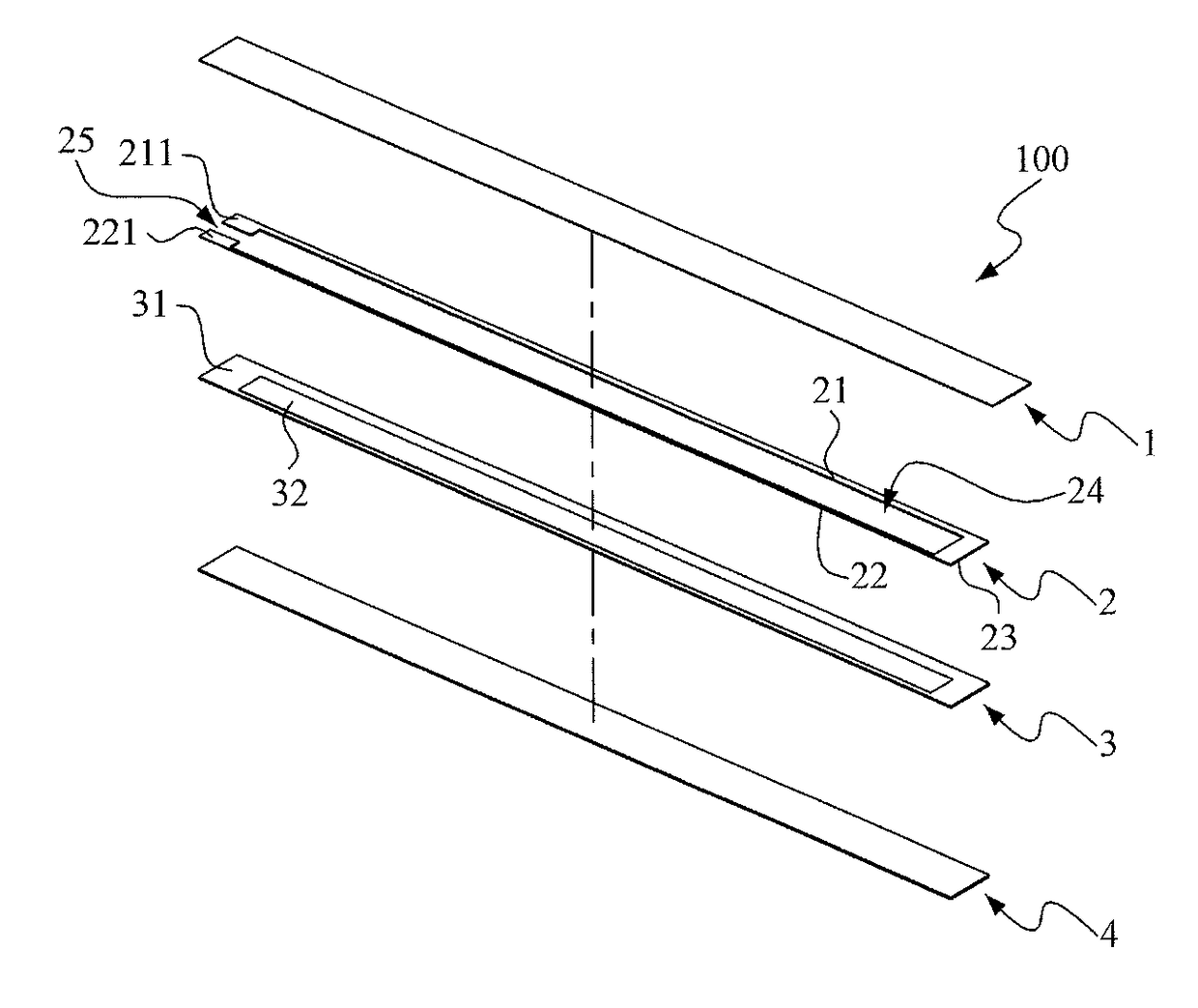
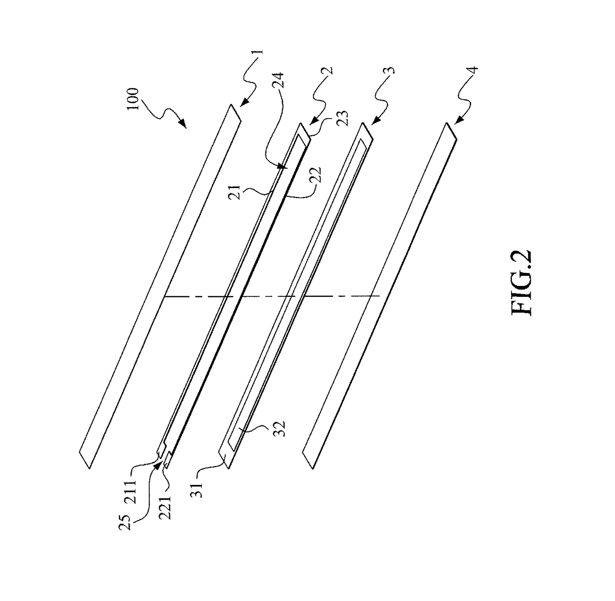
[0038]Refer now to FIG. 2 through FIG. 3A; where FIG. 2 is a schematically exploded view of a preferred embodiment of the bend sensor in accordance with the present invention, FIG. 3 is another view of FIG. 2, and FIG. 3A is an enlarged view of area A of FIG. 3. As shown, the bend sensor 100 includes a flexible circuit substrate 1, an insulation pad 2, a flexible conductive substrate 3 and a reinforcing plate 4.

[0039]The flexible circuit substrate 1 includes an insulating body 11, a first circuit 12 ...


PUM


Abstract

A bend sensor includes a flexible circuit substrate, an insulation pad and a flexible conductive substrate. The flexible circuit substrate includes an insulating body, a first circuit and a second circuit. The first and second circuits are disposed on opposing sides of the insulating body. The first circuit has first fingers, while the second circuit has second fingers. The insulation pad disposed on the insulating body exposes the first and second fingers. The flexible conductive substrate disposed on the insulating pad has a conductive layer separated from the first fingers and the second fingers. While the bend sensor is bent, the conductive layer on the flexible conductive substrate would deform toward the flexible circuit substrate so as to form multiple contacts with the first and second fingers. Through these contacts, a number of resistors are formed to contribute a detectable resistance for the corresponding bending amplitude to be further realized.

Description

BACKGROUND OF THE INVENTION1. Field of the Invention[0001]The invention relates to a bend sensor, and more particularly to the bend sensor that is applied to detect bending amplitudes.2. Description of the Prior Art[0002]Referring now to FIG. 1, a schematically perspective view of a conventional bend sensor is shown. This conventional bend sensor PA100 includes a circuit substrate PA1, a conductive circuit PA2 and a resistance-varying layer PA3. The conductive circuit PA2 and the resistance-varying layer PA3 are both disposed on the circuit substrate PA1, and the conductive circuit PA2 is electrically coupled with one end of the resistance-varying layer PA3. The resistance-varying layer PA3 is formed by alternately arranging conductive sections PA31 and resistor sections PA32. Thereupon, when the bend sensor PA100 is bent, a deformation in a form of extension of the resistor section PA32 would vary significantly the resistance, and the consequent change in the resistance would be im...

Claims


Application Information

Patent Timeline
Patent Type & Authority Applications(United States)
IPC IPC(8): G01D5/16H05K1/02H05K1/11
CPCG01D5/16H05K1/028H05K1/111G01B7/20H05K2201/10151
Inventor HUANG, TZU-HSUANLIU, WEI-LIANGCHAN, HUANG-CHAO
Owner TAIWAN ALPHA ELECTRONICS
Why Eureka
Try Eureka