Chip package structure and manufacturing method thereof

a technology of chip package and manufacturing method, which is applied in the direction of semiconductor devices, electrical devices, semiconductor/solid-state device details, etc., can solve the problems of warpage achieve the effect of enhancing the stiffness and structural strength of the chip package structure, enhancing the stiffness of the reinforcing frame, and high thermal process

Active Publication Date: 2018-04-26
POWERTECH TECHNOLOGY
View PDF2 Cites 4 Cited by
  • Summary
  • Abstract
  • Description
  • Claims
  • Application Information

AI Technical Summary

Benefits of technology

[0008]In light of the foregoing, the chip package structure of the disclosure is subjected to high thermal process, e.g. forming solder balls on the redistribution layer, which may cause warpage of the chip package structure. Accordingly, the reinforcing frame is configured to surround the chip before the redistribution layer and the solder balls are formed. The stiffness of the reinforcing frame is greater than the stiffness of the redistribution layer, so as to enhance the stiffness and structural strength of the chip package structure. Moreover, the warpage of the chip package structure may be reduced, and the reliability of the chip package structure is improved.

Problems solved by technology

In light of the foregoing, the chip package structure of the disclosure is subjected to high thermal process, e.g. forming solder balls on the redistribution layer, which may cause warpage of the chip package structure.

Method used


Image

  • Chip package structure and manufacturing method thereof
  • Chip package structure and manufacturing method thereof
  • Chip package structure and manufacturing method thereof

Examples


Embodiment Construction

[0013]Reference will now be made in detail to the present embodiments of the invention, examples of which are illustrated in the accompanying drawings. Wherever possible, the same reference numbers are used in the drawings and the description to refer to the same or like parts.

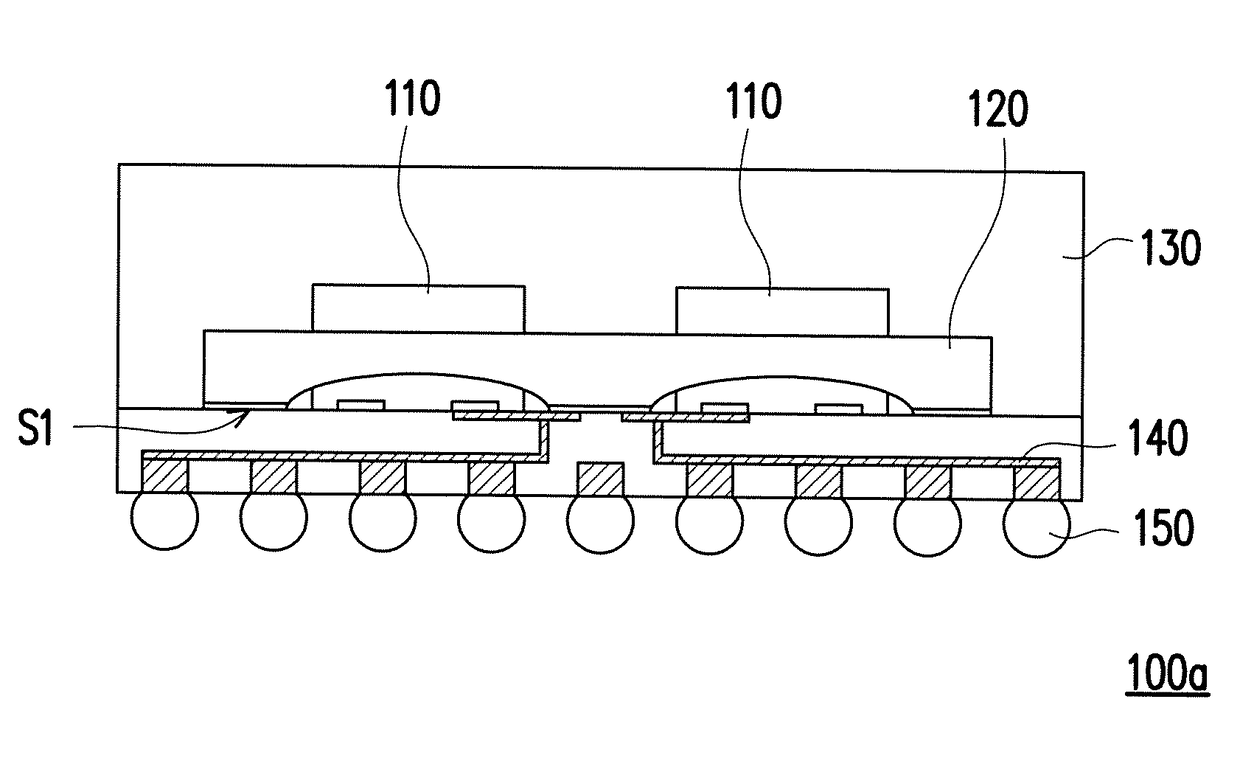
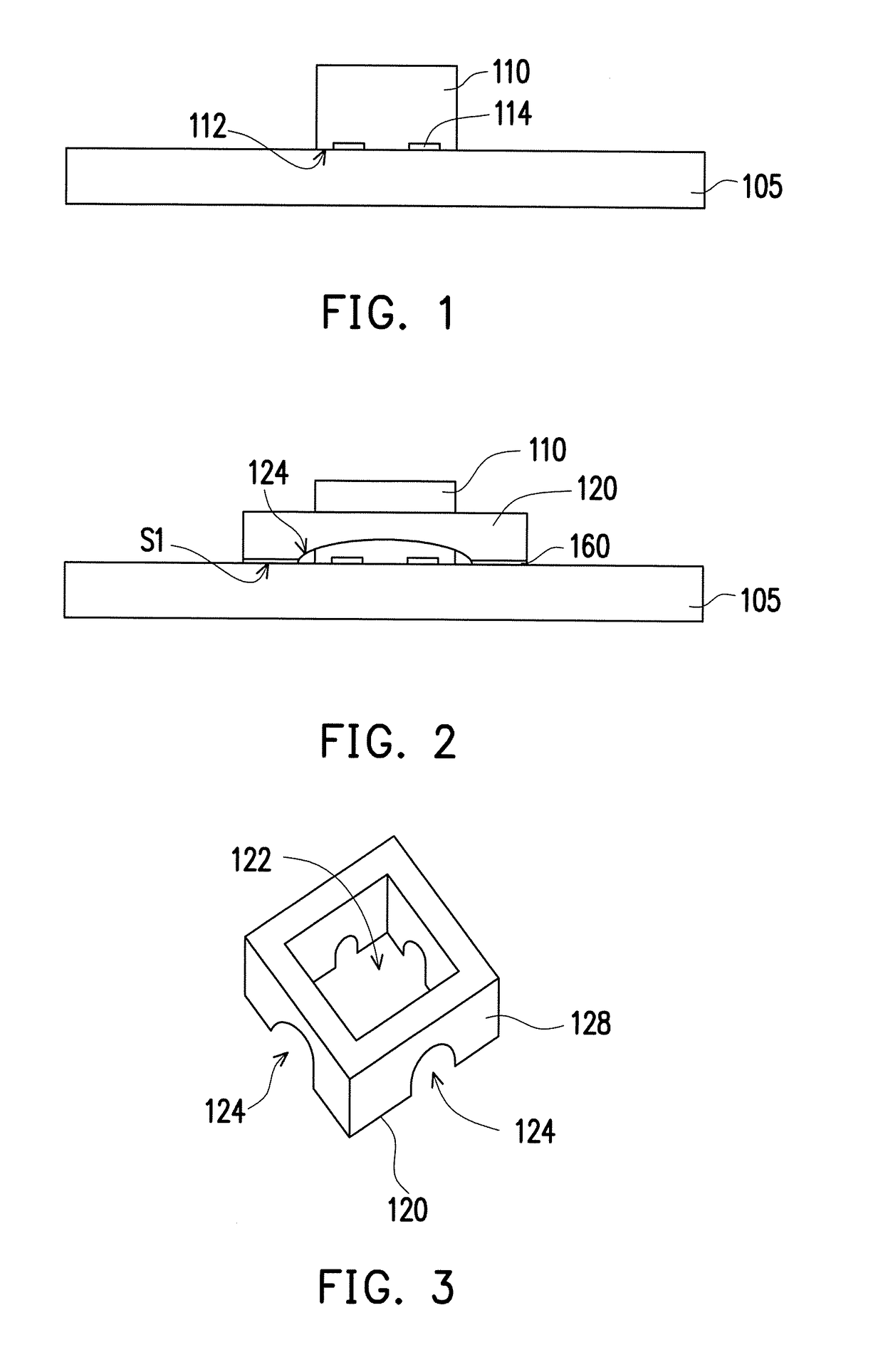
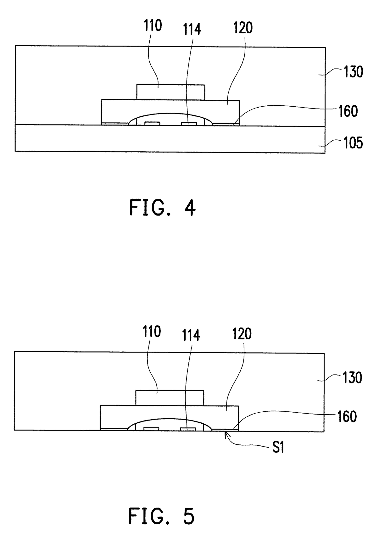
[0014]FIG. 1 to FIG. 7 illustrate a manufacturing method of a chip package structure according to an embodiment of the invention. In the present embodiment, a manufacturing method of a chip package structure includes the following steps. Referring to FIG. 1, at least one chip 110 (one chip is illustrated herein) is disposed on a carrier 105. The chip 110 includes an active surface 112 facing the carrier 105 and a plurality of pads 114 disposed on the active surface 112. In the present embodiment, the chip is mounted on the carrier 105 by a flip-chip bonding technique, but the disclosure is not limited thereto.

[0015]Next, referring to FIG. 2 and FIG. 3, a reinforcing frame 120 as shown in FIG. 3 is disposed on ...


PUM


Abstract

A chip package structure includes a redistribution layer, at least one chip, a reinforcing frame, an encapsulant and a plurality of solder balls. The redistribution layer includes a first surface and a second surface opposite to each other. The chip is disposed on the first surface and electrically connected to the redistribution layer. The reinforcing frame is disposed on the first surface and includes at least one through cavity. The chip is disposed in the through cavity and a stiffness of the reinforcing frame is greater than a stiffness of the redistribution layer. The encapsulant encapsulates the chip, the reinforcing frame and covering the first surface. The solder balls are disposed on the second surface and electrically connected to the redistribution layer.

Description

CROSS REFERENCE TO RELATED APPLICATION[0001]This application claims the priority benefit of U.S. provisional application Ser. No. 62 / 410,853, filed on Oct. 21, 2016. The entirety of the above-mentioned patent application is hereby incorporated by reference herein and made a part of specification.BACKGROUND OF THE INVENTIONField of the Invention[0002]The present invention generally relates to a package structure and manufacturing method thereof. More particularly, the present invention relates to chip package structure and manufacturing method.Description of Related Art[0003]Modern electronic devices require small size, large memory capacity and high performance for their applications such as mobile applications. Consequently, semiconductor chip packages that go into modern electronic devices, such as mobile electronic devices, also have to have small size, large memory capacity, and high performance.[0004]Typically, a printed circuit board (PCB) includes an insulating substrate, whi...

Claims


Application Information

Patent Timeline
Patent Type & Authority Applications(United States)
IPC IPC(8): H01L23/12H01L23/31H01L23/488H01L23/00H01L21/56H01L21/48
CPCH01L23/12H01L23/3114H01L23/488H01L24/26H01L21/56H01L21/4803H01L21/4846H01L21/4817H01L2924/182H01L21/50H01L21/568H01L23/3107H01L23/3135H01L23/49861H01L21/60H01L23/16H01L23/3128H01L23/3142H01L23/49816H01L23/562H01L24/13H01L24/19H01L24/20H01L2224/04105H01L2224/12105H01L2224/131H01L2224/73265H01L2924/181H01L2224/32225H01L2224/48227H01L2924/00H01L2924/014H01L21/2885H01L21/4853H01L21/52H01L21/565H01L23/055H01L23/49827H01L23/49838H01L24/16H01L24/32H01L24/48H01L24/73H01L24/81H01L24/83H01L24/85H01L24/92H01L2021/60022H01L2021/6006H01L2224/16227H01L2224/48091H01L2224/48106H01L2924/17151H01L2924/3511
Inventor WANG, CHI-ANHSU, HUNG-HSINCHANG, WEN-HSIUNG
Owner POWERTECH TECHNOLOGY
Why Eureka
Try Eureka