Optical device

a technology of optical devices and dielectric substrates, applied in non-linear optics, instruments, optics, etc., can solve the problems of increasing manufacturing costs, limited material materials of dielectric substrates, and the material of dielectric substrates, which can be applied, and achieve high-performance optical modulation.

Active Publication Date: 2018-10-04
SUMITOMO OSAKA CEMENT CO LTD
View PDF0 Cites 1 Cited by
  • Summary
  • Abstract
  • Description
  • Claims
  • Application Information

AI Technical Summary

Benefits of technology

[0012]However, in the configuration described in Non-Patent Literature 1, since fine grooves are processed on the dielectric substrate, it leads to an increase in manufacturing cost. Further, in the configuration described in Non-Patent Literature 1, the material of the dielectric substrate, which can be applied, is limited to a material that can maintain mechanical strength even if the grooving is performed. For this reason, the range of choice of the material of the dielectric substrate is narrowed.
[0023]According to the present invention, it is possible to provide an optical device which realizes high-performance optical modulation.

Problems solved by technology

However, in the configuration described in Non-Patent Literature 1, since fine grooves are processed on the dielectric substrate, it leads to an increase in manufacturing cost.
Further, in the configuration described in Non-Patent Literature 1, the material of the dielectric substrate, which can be applied, is limited to a material that can maintain mechanical strength even if the grooving is performed.
Further, the above problem is not limited to the optical modulator using an electro-optic effect and can also likewise occur in an electro-absorption modulator using an electro-absorption effect.

Method used


Image

  • Optical device
  • Optical device
  • Optical device

Examples


Embodiment Construction

[0029]Hereinafter, an optical device 100 according to an embodiment of the present invention will be described with reference to FIG. 1 to FIG. 5. In all of the following drawings, in order to make the drawing easy to see, dimensions, a ratio, or the like of each constituent element is appropriately made different.

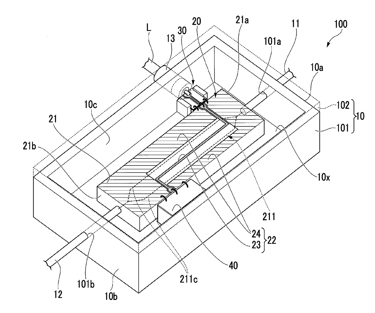
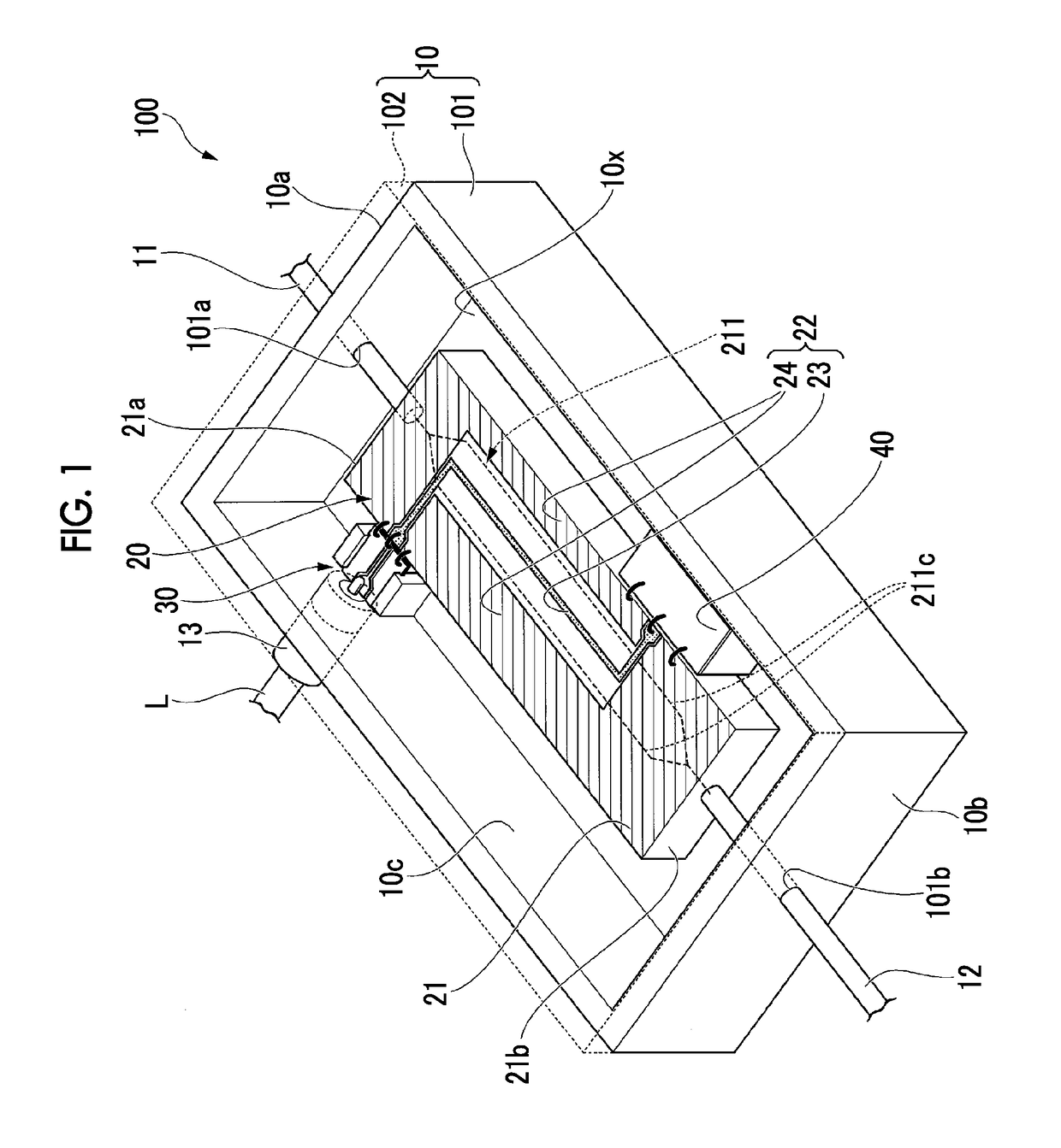
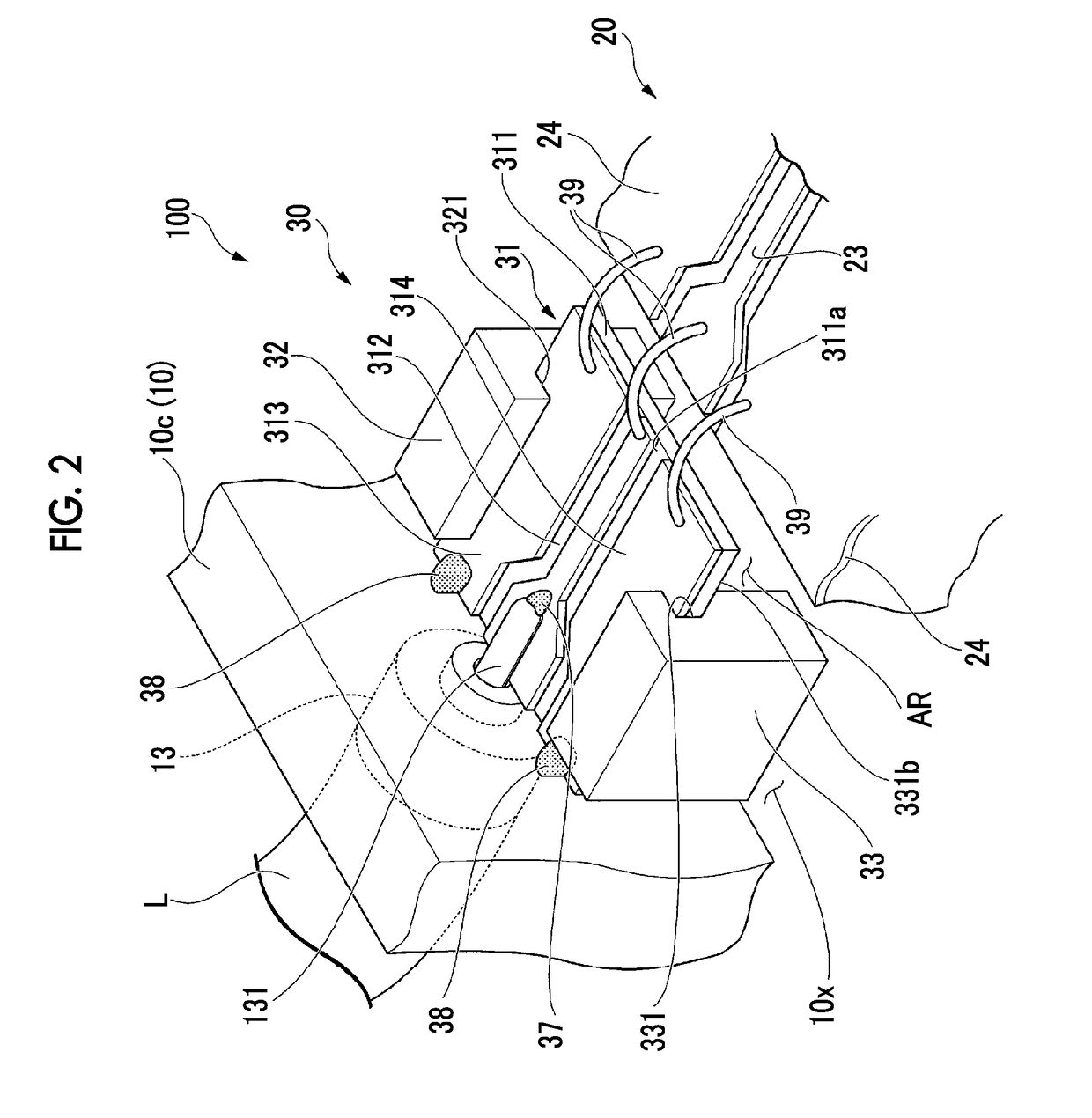
[0030]FIG. 1 is a schematic perspective view showing the optical device 100 of this embodiment. As shown in this drawing, the optical device 100 of this embodiment is an optical modulator having a housing 10, an electro-optical element 20, a relay section 30, and a terminal end section 40.

[0031]Housing

[0032]The housing 10 is a box-shaped member having a rectangular shape when viewed in a plan view and accommodating the electro-optical element 20. The housing 10 has a bottomed case 101 having an open upper portion, and a lid material 102 for closing an opening portion of the upper portion of the case 101.

[0033]A material for forming the housing 10 may be selected according ...


PUM

PropertyMeasurementUnit
relative dielectric constantaaaaaaaaaa
conductiveaaaaaaaaaa
dielectricaaaaaaaaaa

Abstract

An optical device includes: an electro-optical element; a connector for input and output of an electric signal; a relay substrate electrically connecting the connector and the optical element; a pair of support parts supporting the relay substrate; and a housing accommodating the optical element, the relay substrate, and the pair of support parts, in which the optical element includes a substrate having an optical waveguide formed therein, and a modulation electrode formed on a surface of the substrate, the relay substrate includes a dielectric substrate, and a signal electrode and a ground electrode provided on one principal surface of the dielectric substrate, the signal electrode and the ground electrode are electrically connected to the modulation electrode and the connector, the support parts clamps the relay substrate, and an air gap is formed between the other principal surface of the relay substrate and an inner bottom surface of the housing.

Description

CROSS-REFERENCE TO RELATED APPLICATIONS[0001]This application claims the benefit of Japanese Patent Application No. 2017-071632 filed Mar. 31, 2017, the disclosure of which is herein incorporated by reference in its entirety.BACKGROUND OF THE INVENTIONField of the Invention[0002]The present invention relates to an optical device.Description of Related Art[0003]In the related art, as an optical device, an optical modulator having an electro-optical element having an optical waveguide and a modulation electrode, a housing which accommodates the electro-optical element, and a relay substrate which transmits a modulation signal input from the outside to the modulation electrode is known (refer to, for example, Japanese Patent No. 4027109).[0004]The electro-optical element of the optical modulator uses a material exhibiting an electro-optic effect, such as a LiNbO3 crystal or an electro-optical polymer material, as a substrate, and has a configuration in which an optical waveguide is for...

Claims


Application Information

Patent Timeline
Patent Type & Authority Applications(United States)
IPC IPC(8): G02F1/01
CPCG02F1/011G02F1/0316G02F1/0327G02F1/035G02F1/0121G02F1/0344G02F1/2255
Inventor ISHIKAWA, YOSHIZUMITAKANO, SHINGO
Owner SUMITOMO OSAKA CEMENT CO LTD
Why Eureka
Try Eureka