

Semiconductor device and manufacturing method of semiconductor device
a semiconductor device and semiconductor technology, applied in semiconductor devices, semiconductor/solid-state device details, inductance, etc., can solve the problems of not providing devices which make full use of flexible substrates, preventing device flexibility, and reducing so as to reduce damage to the element formation layer, maintain the mechanical strength of semiconductor devices, and ensure the effect of flexibility
- Summary
- Abstract
- Description
- Claims
- Application Information
AI Technical Summary
Benefits of technology
Problems solved by technology
Method used
Image

Examples
embodiment mode 1
[0040] Embodiment Mode 1 will explain an example of a semiconductor device of the present invention with reference to drawings.
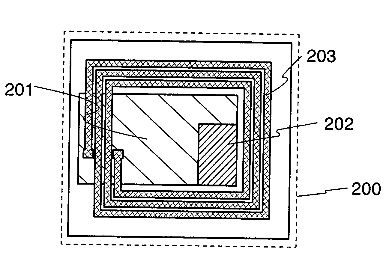
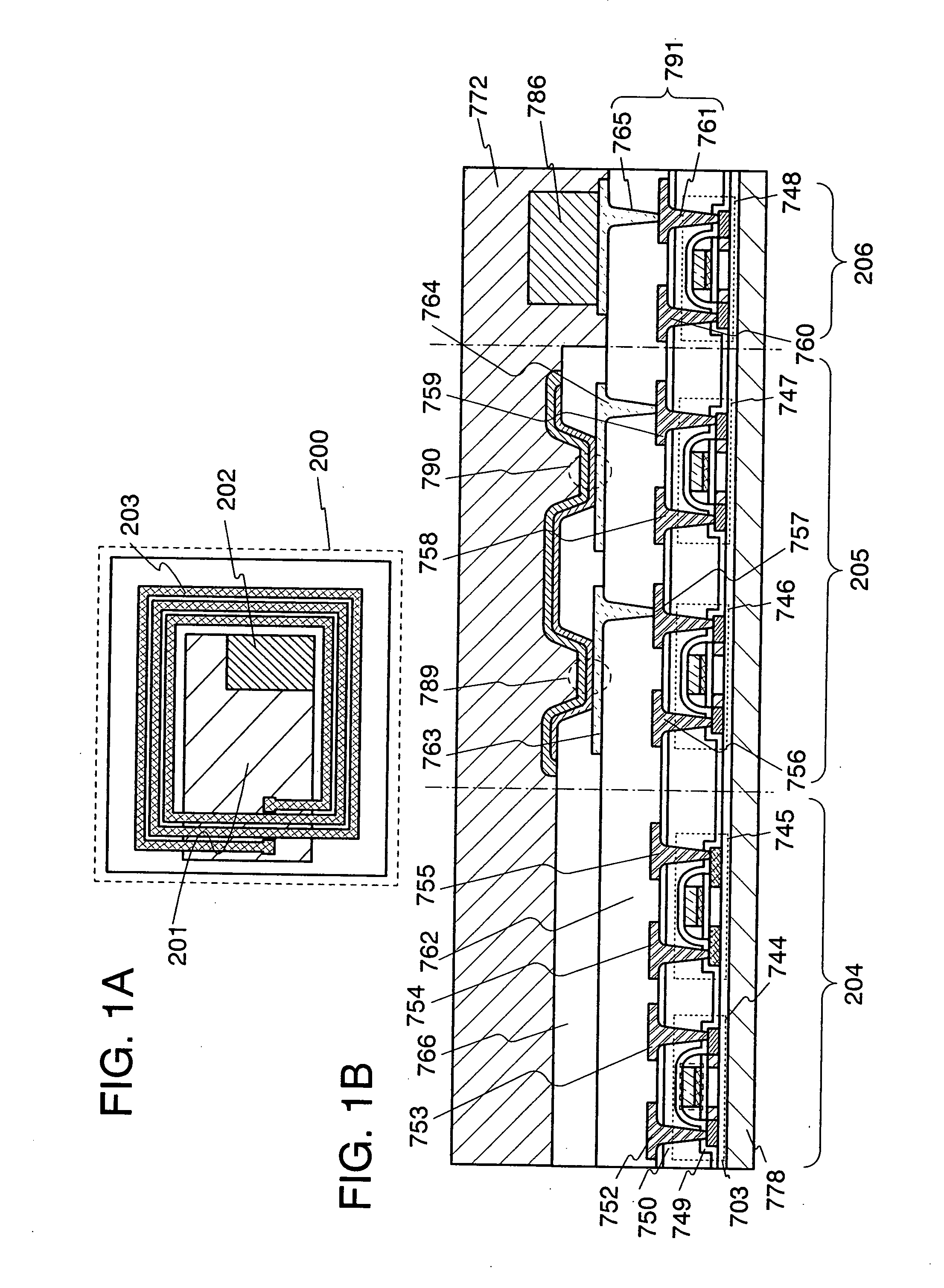
[0041]FIGS. 1A and 1B show a semiconductor device of this embodiment mode. Note that FIG. 1A illustrates an example of a top face structure of the semiconductor device shown in this embodiment mode, and FIG. 1B illustrates a part of a cross-sectional structure of FIG. 1A.
[0042] In this embodiment mode, a semiconductor device 200 includes an integrated circuit portion 201, a memory section 202 and an antenna 203 (FIG. 1A). In FIG. 1B, a region 204 corresponds to a part of the cross-sectional structure of the integrated circuit portion 201 of FIG. 1A, a region 205 corresponds to a part of the cross-sectional structure of the memory section 202 of FIG. 1A, and a region 206 corresponds to a part of the cross-sectional structure of the antenna 203 of FIG. 1A.
[0043] The semiconductor device of this embodiment mode includes thin film transistors (TFTs) 744 to 74...
embodiment mode 2
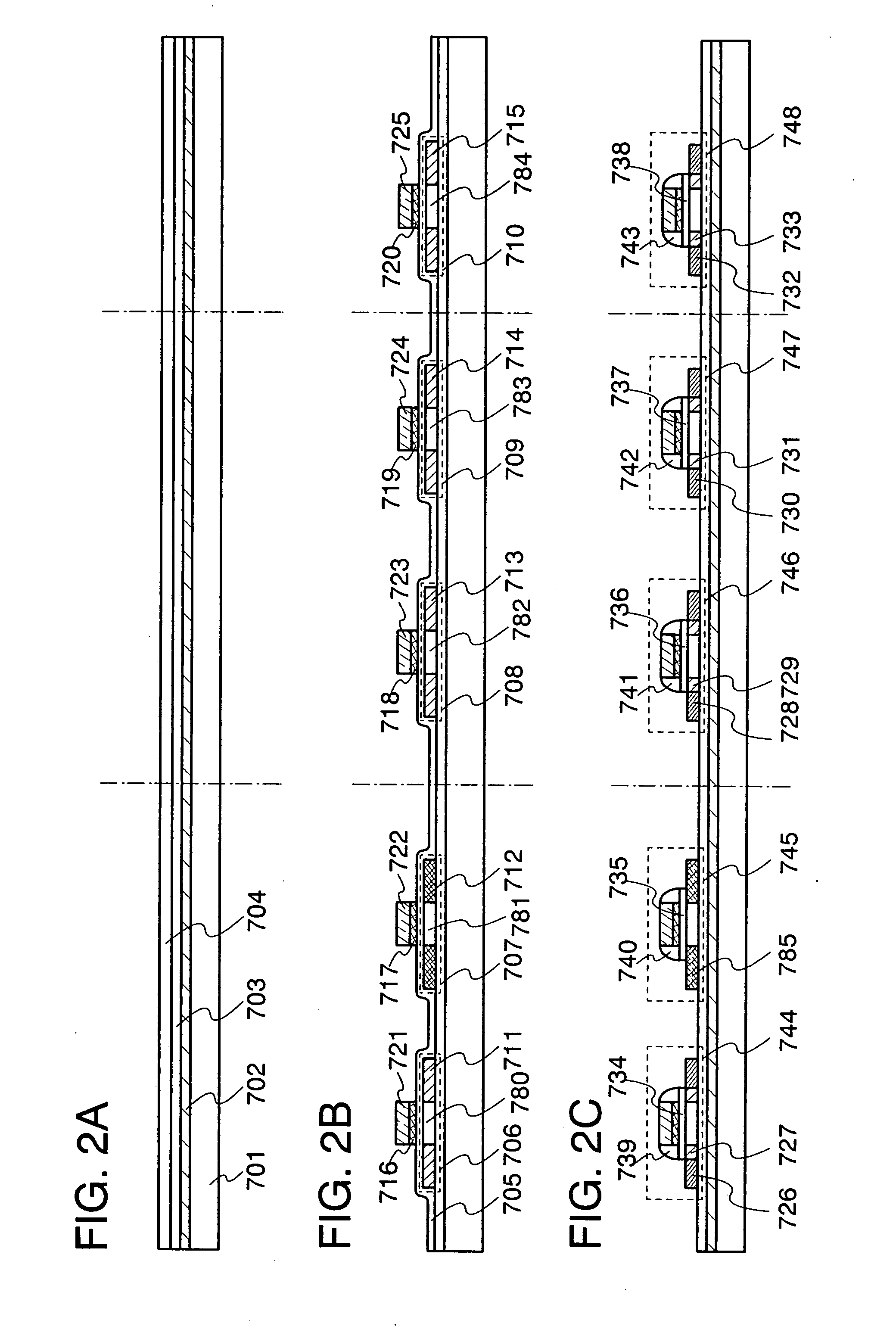
[0109] Embodiment Mode 2 will describe a manufacturing process of a semiconductor device which is different from that of Embodiment Mode 1. Specifically, a process is described in which a pn junction of a memory cell and a thin film transistor of a logic portion for controlling the memory cell are formed at the same time.
[0110]FIG. 7 shows a schematic cross-sectional structure of a semiconductor device of this embodiment mode. The semiconductor device of this embodiment mode includes an antenna, a memory section, and an integrated circuit portion. The cross section of the memory cell as a part of the memory section is shown in the center of FIG. 7. In the memory cell, a storage element portion is stacked over a diode as a part of the memory section. The left part of the drawing shows a cross section of a p-channel TFT (also referred to as a p-ch TFT) and an n-channel TFT (also referred to as an n-ch TFT) as a part of the cross section of the logic circuit in the memory section. The...
embodiment mode 3
[0146] Embodiment Mode 3 will explain an example of applying a semiconductor device of the present invention to a semiconductor device capable of inputting and outputting data without contact with reference to drawings. The semiconductor device capable of inputting and outputting data without contact is also referred to as an RFID (Radio Frequency Identification) tag, an ID tag, an IC tag, an IC chip, an RF tag, a wireless tag, an electronic tag, or a wireless chip.
[0147]FIG. 12 is a block diagram showing a structure example of a semiconductor device 200 of this embodiment mode. The semiconductor device 200 has an antenna 210 to exchange data without contact (wirelessly). The semiconductor device 200 further includes a resonance circuit 212, a power source circuit 213, a reset circuit 214, a clock generating circuit 215, a data demodulating circuit 216, a data modulating circuit 217, a control circuit 220 for controlling another circuit, and a memory section 230, as signal processi...
PUM
 Abstract
Description
Claims
Application Information