Electronic device
a technology of electronic devices and terminal electrodes, applied in the direction of fixed capacitor details, stacked capacitors, fixed capacitors, etc., can solve the problems of deterioration of acoustic noise, insufficient reliability of the connection part between the terminal electrode of the chip device and the external terminal, and increase of equivalent series resistance (esr)
- Summary
- Abstract
- Description
- Claims
- Application Information
AI Technical Summary
Benefits of technology
Problems solved by technology
Method used
Image
Examples
first embodiment
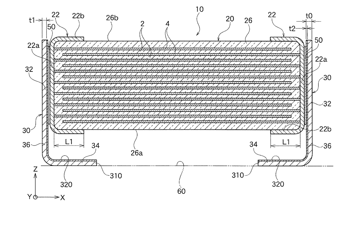
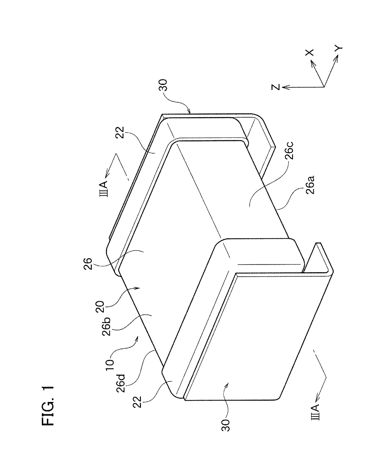
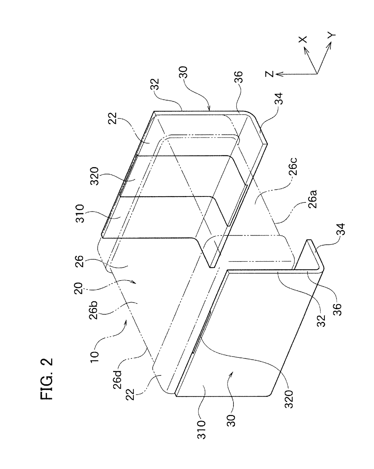
[0044]FIG. 1 is a schematic cross-sectional view showing an electronic device 10 according to First Embodiment of the present invention. The electronic device 10 has a chip capacitor 20 as a chip component and a pair of metal terminals (external terminals) 30 respectively attached on both end surfaces of the chip capacitor 20 in the X-axis direction.
[0045]Incidentally, each embodiment is explained based on an electronic device where a pair of metal terminals 30 is attached on the chip capacitor 20, but the present invention is not limited to this electronic device, and may be an electronic device where the metal terminals 30 are attached to a chip component other than a capacitor.
[0046]The chip capacitor 20 has a capacitor element body (ceramic element body) 26 and a pair of terminal electrodes 22 respectively formed on both end surfaces of the capacitor element body 26 in the X-axis direction. The capacitor element body 26 has four side surfaces 26a, 26b, 26c, and 26d, all of which...
second embodiment
[0092]FIG. 4 is a perspective view of an electronic device 10A according to Second Embodiment of the present invention. The electronic device 10A according to the present embodiment has the same structure and demonstrates the same effect as the electronic device 10 according to First Embodiment shown in FIG. 1 to FIG. 3A except for the following description. Thus, common members are provided with common parts numbers and are not described.
[0093]In the present embodiment, as shown in FIG. 4, a second metal 320A is formed only on a part of a metal terminal 30A corresponding to the terminal electrode connection part 32, and the mount connection part 34 and the coupled part 36 are formed by only the first metal 310. The other structure is similar to the above-mentioned embodiment, and similar effects are demonstrated.
third embodiment
[0094]FIG. 5A and FIG. 5B are a perspective view of an electronic device 10B according to Third Embodiment of the present invention. The electronic device 10B according to the present embodiment has similar structure and effects to the electronic device 10 according to First Embodiment shown in FIG. 1 to FIG. 3A except for the following description. Thus, common members are provided with common parts numbers and are not described.
[0095]In the present embodiment, as shown in FIG. 5A and FIG. 5B, a metal terminal 30B has a first metal 310 and a second metal 320, and the first metal 310 and the second metal 320 are alternately exposed on a surface of the metal terminal 30B (outward in the Y-axis direction) opposite to its surface facing the end surface of the capacitor element body 26. Incidentally, only the first metal 310 is exposed on the surface of the metal terminal 30B facing the end surface of the capacitor element body 26, and only the first metal 310 is directly connected with...
PUM
| Property | Measurement | Unit |
|---|---|---|
| Electrical resistance | aaaaa | aaaaa |
Abstract
Description
Claims
Application Information


