Touch Control Structure of an Active-Matrix Organic Light-Emitting Diode Display Screen

a technology of organic light-emitting diodes and display screens, which is applied in the field of touch control technology, can solve the problems of encapsulation making on oled device differences huge, in-cell technology very difficult to be applied to oled device, etc., and achieves the effect of reducing process difficulty and minimizing adverse effects

Active Publication Date: 2019-01-17
KUNSHAN NEW FLAT PANEL DISPLAY TECH CENT +1
View PDF6 Cites 2 Cited by
  • Summary
  • Abstract
  • Description
  • Claims
  • Application Information

AI Technical Summary

Benefits of technology

[0004]In order to solve the problem in prior art by minimizing the adverse influence of multiple times of photo-etching on the film encapsulation and reducing the degree of difficulty of the process, the present invention provides a touch control structure of an active-matrix organic light-emitting diode display screen.
[0020](1) In the present invention, the first encapsulation film and the second encapsulation film together constitute an encapsulation layer for the active-matrix organic light-emitting diode display screen, and the first patterned electrode of the touch control structure is embedded within this encapsulation layer. Therefore, not only the organic light-emitting diode device of the display screen can be protected by this encapsulation layer from moisture and oxygen corrosion, but also, with the first patterned electrode of the touch control structure embedded within this encapsulation layer, the overall thickness of the touch control display screen can be significantly reduced.
[0021](2) In the present invention, a first patterned electrode and a second patterned electrode are respectively formed on the first encapsulation film and on the flexible polymer foil, and thus these patterned electrodes can be made from nano silver or grapheme with low cost, which further reduces the cost and at the same time achieves flexible touch control.
[0022](3) In the present invention, the receiving structure is formed on the basis of a flexible polymer foil sheet which is made from materials including but not limited to polyethylene terephthalate, polyethylene terenaphthalate, polyethersulfone, polyimide and parylene, the second patterned electrode of the capacitive touch control sensor is formed on the polymer foil sheet, and the second patterned electrode has the same material, forming method and selection range as those of the first patterned electrode. Because the second patterned electrode is formed directly upon the flexible polymer foil sheet, not upon a device component, the degree of difficulty of the manufacture process is significantly reduced.

Problems solved by technology

As for a flexible active-matrix organic light-emitting diode (AMOLED) display screen, the existence of film encapsulation makes the on-cell technology very hard to be applied, because forming a conventional touch control structure on the film encapsulation requires multiple times of photo-etching which have significant adverse influence on the OLED device beneath the film encapsulation.
An OLED device has huge differences from a liquid crystal display device, which makes the in-cell technology very hard to be applied to an OLED device.

Method used


Image

  • Touch Control Structure of an Active-Matrix Organic Light-Emitting Diode Display Screen
  • Touch Control Structure of an Active-Matrix Organic Light-Emitting Diode Display Screen

Examples


embodiment 1

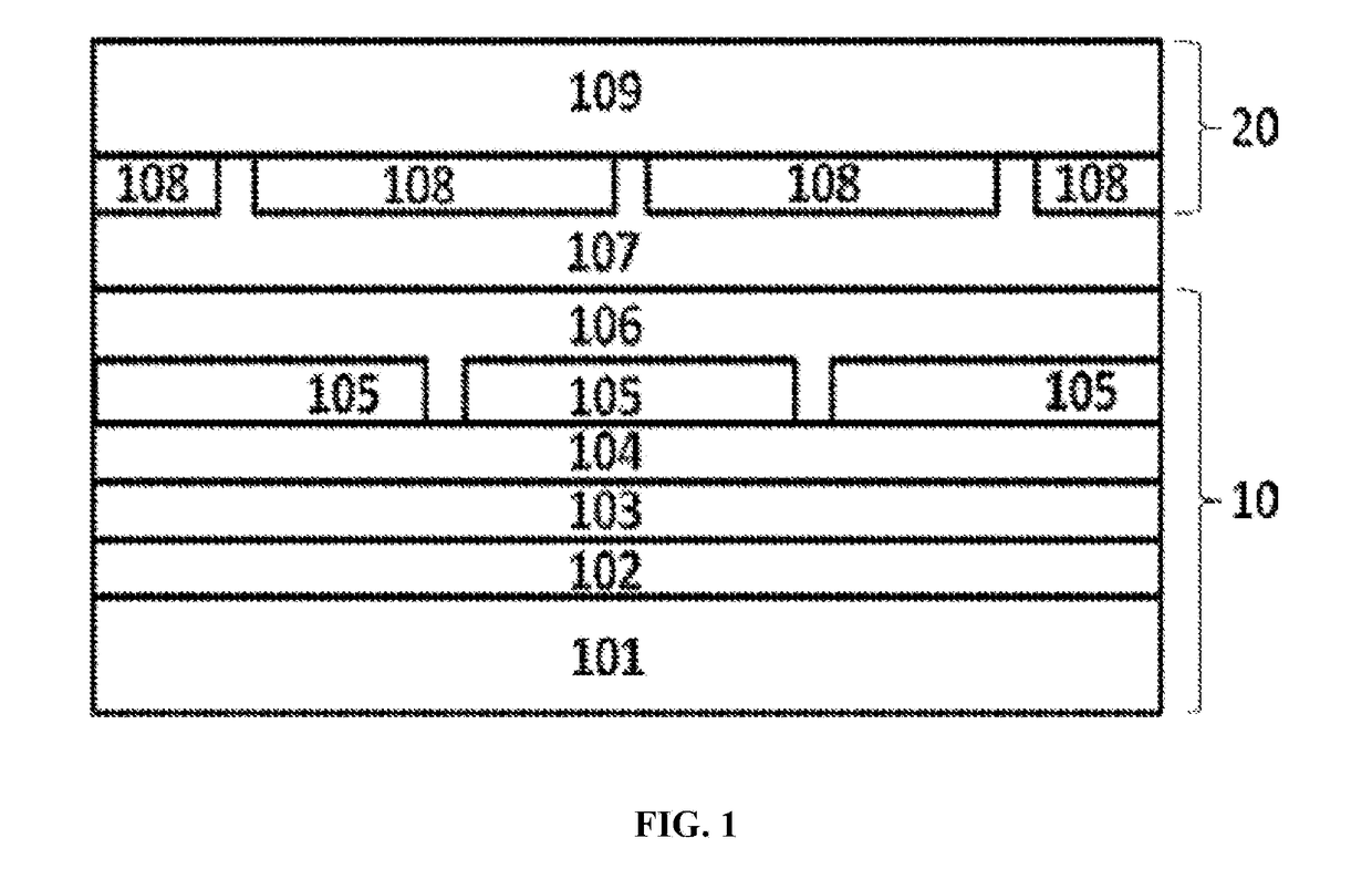
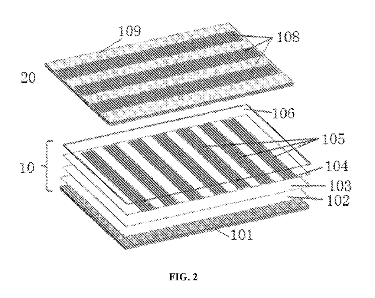
[0040]As shown in FIG. 2, the display screen substrate 101 is a flexible polymer substrate made from polyimide. A low temperature polycrystalline silicon thin film transistor array is formed on the display screen substrate, and then an organic light-emitting diode device 103 is formed upon the top electrodes corresponding to this array. The first encapsulation film 104 is composed of alternately formed two pairs of polyacrylate layers and silicon nitride layers, wherein the silicon nitride layer is produced by plasma enhanced chemical vapor deposition and the polyacrylate layer is produced by ink-jet printing followed by ultraviolet curing. The first patterned electrode 105 of the capacitive touch control sensor is formed on the first encapsulation film 104, wherein the first patterned electrode 105 has a bar-shaped pattern and a thickness of 25 nm and is made from indium tin oxide by a preparation method of magnetron sputtering and a patterning method of metal mask. The second enca...


PUM


Abstract

The present invention discloses a touch control structure of an active-matrix organic light-emitting diode display screen, comprising a transmitting structure and a receiving structure that are mutually inductive, the transmitting structure comprises a first encapsulation film, a first patterned electrode and a second encapsulation film; the receiving structure further comprises a flexible polymer foil sheet and a second patterned electrode formed on the flexible polymer foil sheet, the receiving structure and the transmitting structure are assembled by adhering the surface of the flexible polymer foil sheet having the second patterned electrode formed thereon to the second encapsulation film; wherein, the first encapsulation film comprises multiple layers of films including at least one layer of inorganic film, the second encapsulation film comprises multiple layers of films including at least one layer of inorganic film.

Description

[0001]This application is a continuation of U.S. utility application Ser. No. 15 / 102,719, with a filing date Jun. 8, 2016, which is national stage entry (371) of International Patent Application No. PCT / CN2014 / 093359 with a filing date of Dec. 9, 2014, designating the United States, and further claims priority to Chinese Patent Application No. 201320801754.8 with a filing date of Dec. 9, 2013. The content of the aforementioned applications, including any intervening amendments thereto, are incorporated herein by reference.TECHNICAL FIELD[0002]The present invention relates to the field of display panels and touch control technology, more specifically, the present invention relates to a touch control structure of an active-matrix organic light-emitting diode (AMOLED) display screen which is a hybrid touch control structure.BACKGROUND OF THE INVENTION[0003]Touch control has become a necessary configuration of small to medium display panels and has a large market. In order to increase t...

Claims


Application Information

Patent Timeline
Patent Type & Authority Applications(United States)
IPC IPC(8): G06F3/041H01L27/32G06F3/044
CPCG06F2203/04102G06F2203/04103G09G2300/0426G06F3/0446G06F3/0445H10K59/40G06F3/0412H10K59/12
Inventor ZHU, SHAOPENGHIRAYAMA, HIDEOHUANG, XIUQI
Owner KUNSHAN NEW FLAT PANEL DISPLAY TECH CENT
Why Eureka
Try Eureka