Electronic component
a technology of electronic components and components, applied in the direction of transformer/inductance details, inductances, fixed inductances, etc., can solve the problems of reducing the electric resistance of the interlayer, and achieve the effect of reducing the peeling more effectively, and reducing the peeling of the interlayer
- Summary
- Abstract
- Description
- Claims
- Application Information
AI Technical Summary
Benefits of technology
Problems solved by technology
Method used
Image

Examples
first embodiment
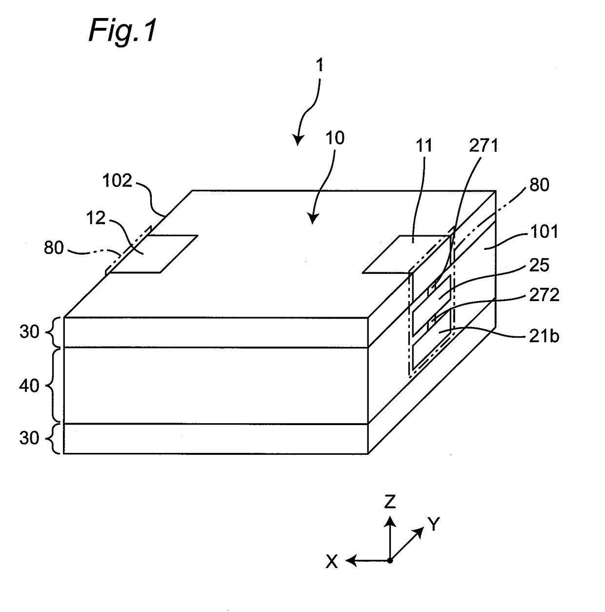
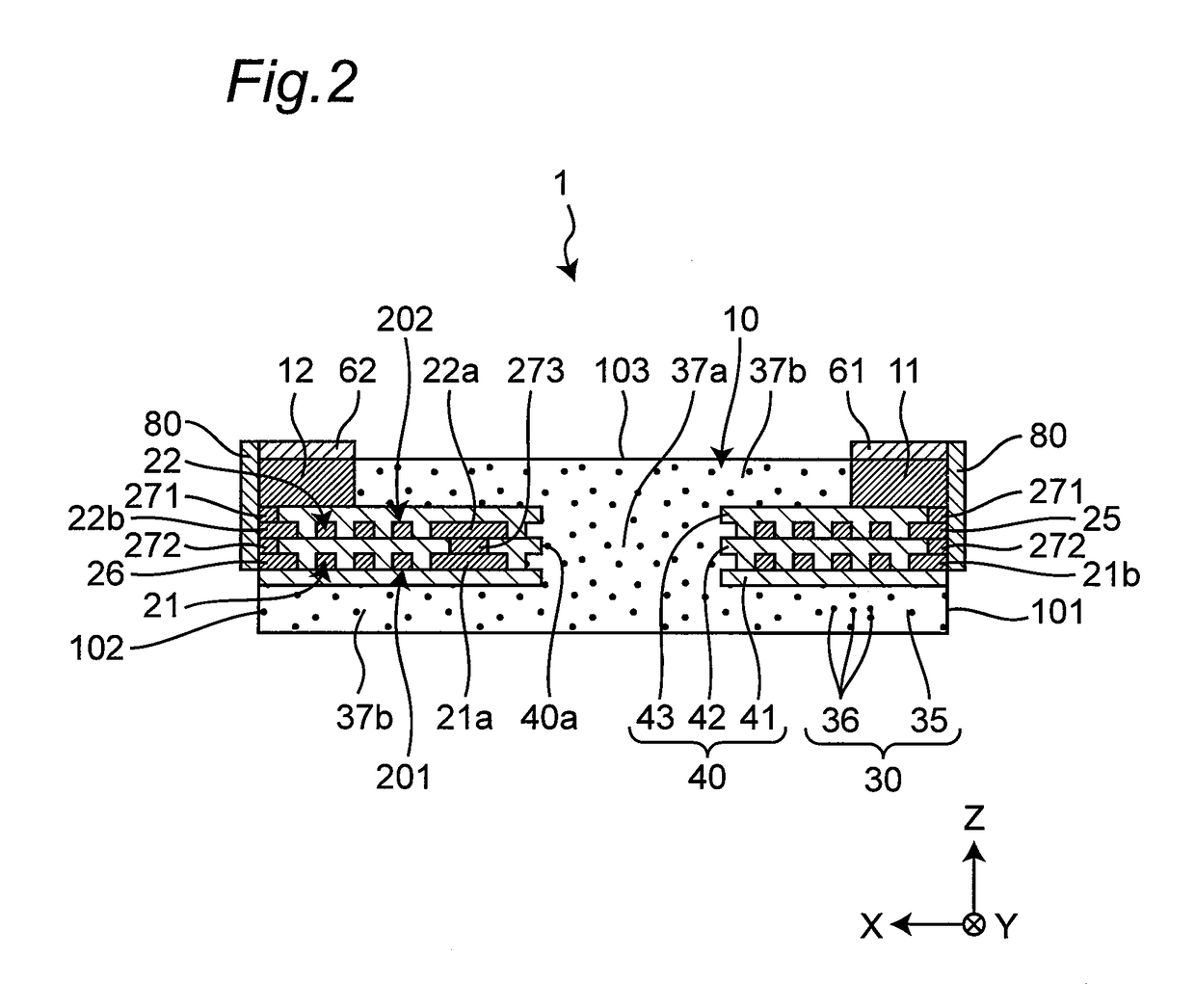
[0039]FIG. 1 is a perspective view of a first embodiment of an electronic component. FIG. 2 is an XZ cross-sectional view of the electronic component. FIGS. 1 and 2 show a coil component 1 as an example of an electronic component. The coil component 1 is mounted on an electronic device such as a personal computer, a DVD player, a digital camera, a TV, a portable telephone, and automotive electronics, for example, and is a component generally having a rectangular parallelepiped shape, for example. However, the shape of the coil component 1 is not particularly limited and may be a circular columnar shape, a polygonal columnar shape, a truncated cone shape, or a truncated polygonal pyramid shape.
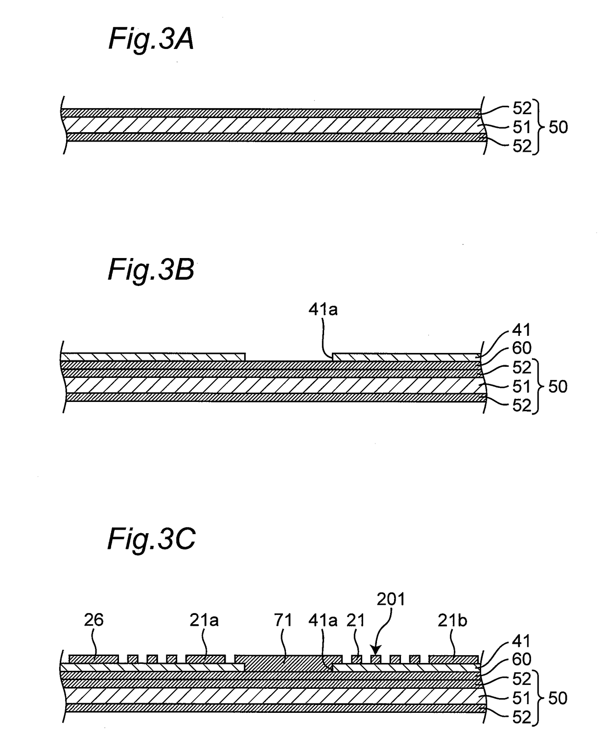
[0040]As shown in FIGS. 1 and 2, the coil component 1 has a main body part 10 including insulating layers 41, 42, 43 and conductor layers 201, 202 laminated alternately, and external electrodes 61, 62 disposed on one surface 103 in a lamination direction of the main body part 10 and electricall...
second embodiment
[0085]FIG. 4 is a view on X-direction arrow of a second embodiment of an electronic component of the present disclosure. The second embodiment is different from the first embodiment in the configuration of the via electrodes. This different configuration will hereinafter be described. In the second embodiment, the same constituent elements as the first embodiment are denoted by the same reference numerals as the first embodiment and therefore will not be described.
[0086]As shown in FIG. 4, in a coil component 1A serving as the electronic component, a width of a first via electrode 271A on one side in the lamination direction is smaller than a width of the first via electrode 271A on the other side in the lamination direction. Specifically, a width of a lower end (the lower side in the Z direction) of the first via electrode 271A is smaller than a width of an upper end (the upper side in the Z direction) of the first via electrode 271A. Therefore, the shape of the first via electrode...
third embodiment
[0089]FIG. 5 is a perspective view of a third embodiment of an electronic component of the present disclosure. The third embodiment is different from the first embodiment in the numbers of external electrodes and metal films. This different configuration will hereinafter be described. In the third embodiment, the same constituent elements as the first embodiment are denoted by the same reference numerals as the first embodiment and therefore will not be described.
[0090]As shown in FIG. 5, in a coil component 1B serving as the electronic component, the multiple (in this embodiment, four) first external electrodes 61 are arranged in parallel along the Y direction on the one surface 103 of the main body part 10. The multiple (in this embodiment, four) metal films 80 are arranged in parallel along the Y direction on the first side surface 101 of the main body part 10. The first external electrodes 61 are respectively connected to the metal films 80.
[0091]Similarly, the multiple (in this...
PUM
| Property | Measurement | Unit |
|---|---|---|
| width | aaaaa | aaaaa |
| insulating | aaaaa | aaaaa |
| conductor | aaaaa | aaaaa |
Abstract
Description
Claims
Application Information
 - R&D Engineer
- R&D Manager
- IP Professional
- Industry Leading Data Capabilities
- Powerful AI technology
- Patent DNA Extraction
Browse by: Latest US Patents, China's latest patents, Technical Efficacy Thesaurus, Application Domain, Technology Topic.
© 2024 PatSnap. All rights reserved.Legal|Privacy policy|Modern Slavery Act Transparency Statement|Sitemap