Electronic device

a technology of electronic devices and components, applied in the field of electronic devices, can solve the problems of limiting the restoration of calculation results, information gaps, and difficulty in achieving the balance between the two conventional technologies

Active Publication Date: 2019-04-04
LARGAN PRECISION
View PDF0 Cites 22 Cited by
  • Summary
  • Abstract
  • Description
  • Claims
  • Application Information

AI Technical Summary

Benefits of technology

[0006]According to one aspect of the present disclosure, an electronic device includes at least one optical lens assembly. The optical lens assembly includes four lens elements, and the four lens elements are, in order from an outside to an inside, a first lens element, a second lens element, a third lens element and a fourth lens element. The first lens element has an outside surface being convex in a paraxial region thereof. The second lens element has an inside surface being convex in a paraxial region thereof. The fourth lens element has an inside surface being concave in a paraxial region thereof, wherein at least one of an outside surface and the inside surface of the fourth lens element includes at least one critical point in an off-axis region thereof. When a measurement is made in accordance with a reference wavelength as a d-line, an Abbe number of the first lens element is Vd1, an Abbe number of the second lens element is Vd2, an Abbe number of the third lens element is Vd3, an Abbe number of the fourth lens element is Vd4, a focal length of the optical lens assembly is fd, a focal length of the third lens element is fd3, and a focal length of the fourth lens element is fd4, the following conditions are satisfied:
[0007]According to one aspect of the present disclosure, an electronic device includes at least one optical lens assembly. The optical lens assembly includes four lens elements, and the four lens elements are, in order from an outside to an inside, a first lens element, a second lens element, a third lens element and a fourth lens element. The second lens element has an outside surface being concave in a paraxial region thereof and an inside surface being convex in a paraxial region thereof. The third lens element has an outside surface being concave in a paraxial region thereof. The fourth lens element has an outside surface being convex in a paraxial region thereof and an inside surface being concave in a paraxial region thereof, wherein the outside surface of the fourth lens element includes at least one critical point in an off-axis region thereof. At least one of the third lens element and the fourth lens element has positive refractive power, and the other one has negative refractive power. When a measurement is made in accordance with a reference wavelength as a d-line, an Abbe number of the first lens element is Vd1, an Abbe number of the second lens element is Vd2, an Abbe number of the third lens element is Vd3, an Abbe number of the fourth lens element is Vd4, a focal length of the optical lens assembly is fd, a focal length of the third lens element is fd3, and a focal length of the fourth lens element is fd4, the following conditions are satisfied:
[0008]According to one aspect of the present disclosure, an electronic device is includes a sensing module, which includes a projection apparatus and a receiving apparatus. The projection apparatus includes an optical lens assembly and at least one light source, wherein the optical lens assembly includes four to six lens elements, and the light source is disposed on an inside conjugation surface of the optical lens assembly. The receiving apparatus includes an optical lens assembly and an image sensor, wherein the optical lens assembly includes four to six lens elements, and the image sensor is disposed on an inside conjugation surface of the optical lens assembly. The light source of the projection apparatus is projected on a sensed object and is received by the receiving apparatus after a reflection, and is imaged on the image sensor. When a measurement is made in accordance with a reference wavelength as a d-line, at least six lens elements of the lens elements of the optical lens assembly of the projection apparatus and the lens elements of the optical lens assembly of the receiving apparatus have Abbe numbers smaller than 38. In the optical lens assembly of each of the projection apparatus and the receiving apparatus, an axial distance between an outside surface of one of the lens elements closest to the outside and an inside surface of one of the lens elements closest to the inside is TD, and the following condition is satisfied:

Problems solved by technology

Conventional three-dimensional space identification technologies are mostly limited to two-dimensional images, and can achieve three-dimensional spatial analysis functions with algorithms, however, when information of three-dimensional space of information is simplified into the two-dimensional space image, it will always result in information gaps, and limit restore results of calculation.
However, with applications, such as face recognition and augmented reality, being used in portable devices, such as smart phones are gradually developed, the sensing module thereof needs to be more precise and compact, but conventional technologies are still difficult to achieve the balance between the two.

Method used


Image

  • Electronic device
  • Electronic device
  • Electronic device

Examples


1st embodiment

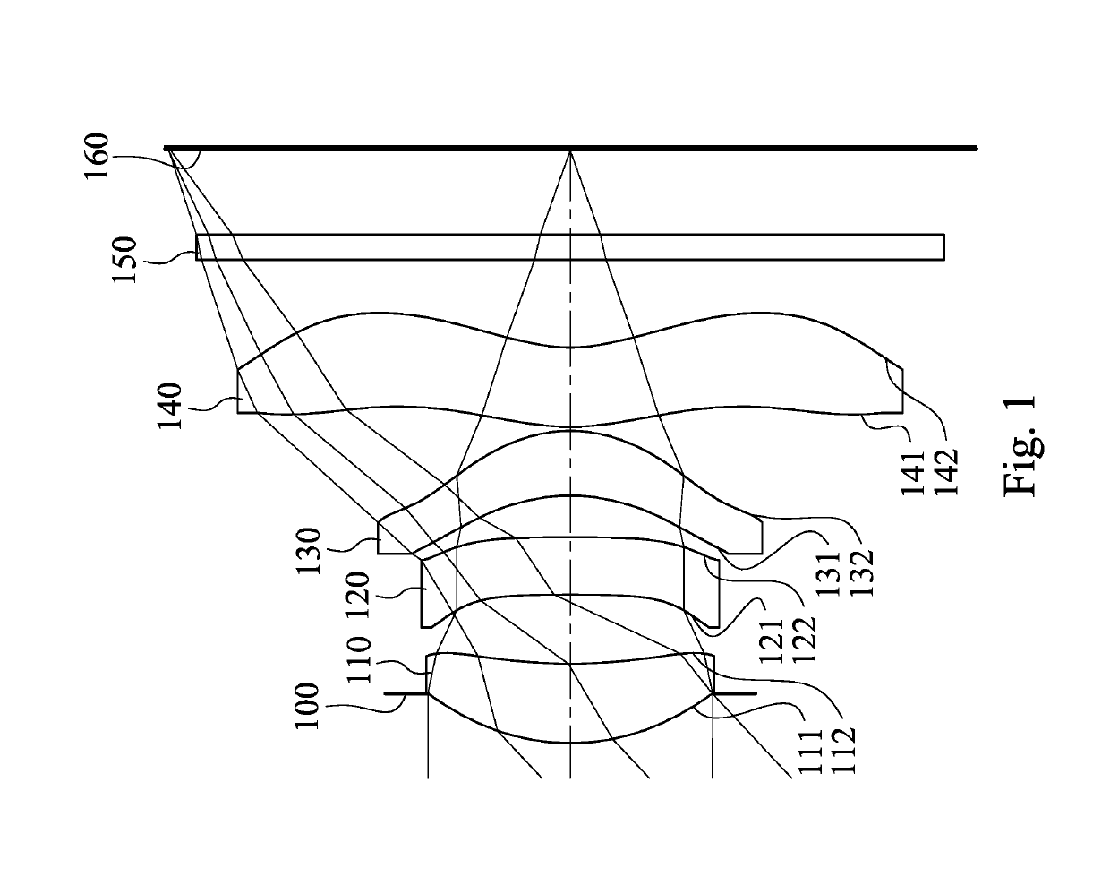
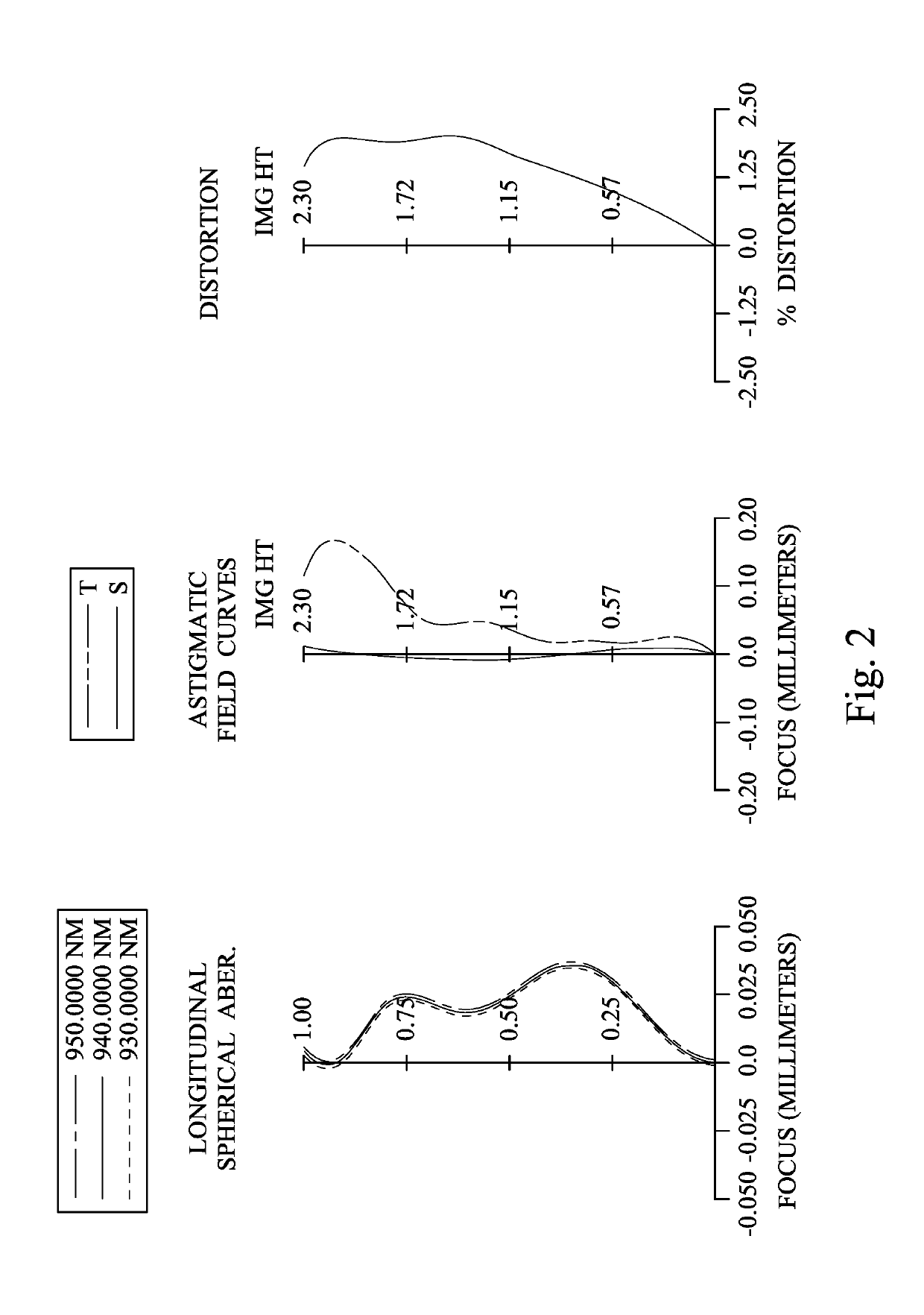
[0090]FIG. 1 is a schematic view of an electronic device according to the 1st embodiment of the present disclosure. FIG. 2 shows spherical aberration curves, astigmatic field curves and a distortion curve of the electronic device according to the 1st embodiment. In FIG. 1, the electronic device includes an optical lens assembly (its reference numeral is omitted), wherein the optical lens assembly includes, in order from an outside to an inside, an aperture stop 100, a first lens element 110, a second lens element 120, a third lens element 130, a fourth lens element 140, a filter 150 and an inside conjugation surface 160. The optical lens assembly includes four lens elements (110, 120, 130 and 140) without additional one or more lens elements inserted between the first lens element 110 and the fourth lens element 140.

[0091]The first lens element 110 with positive refractive power has an outside surface 111 being convex in a paraxial region thereof and an inside surface 112 being conc...

2nd embodiment

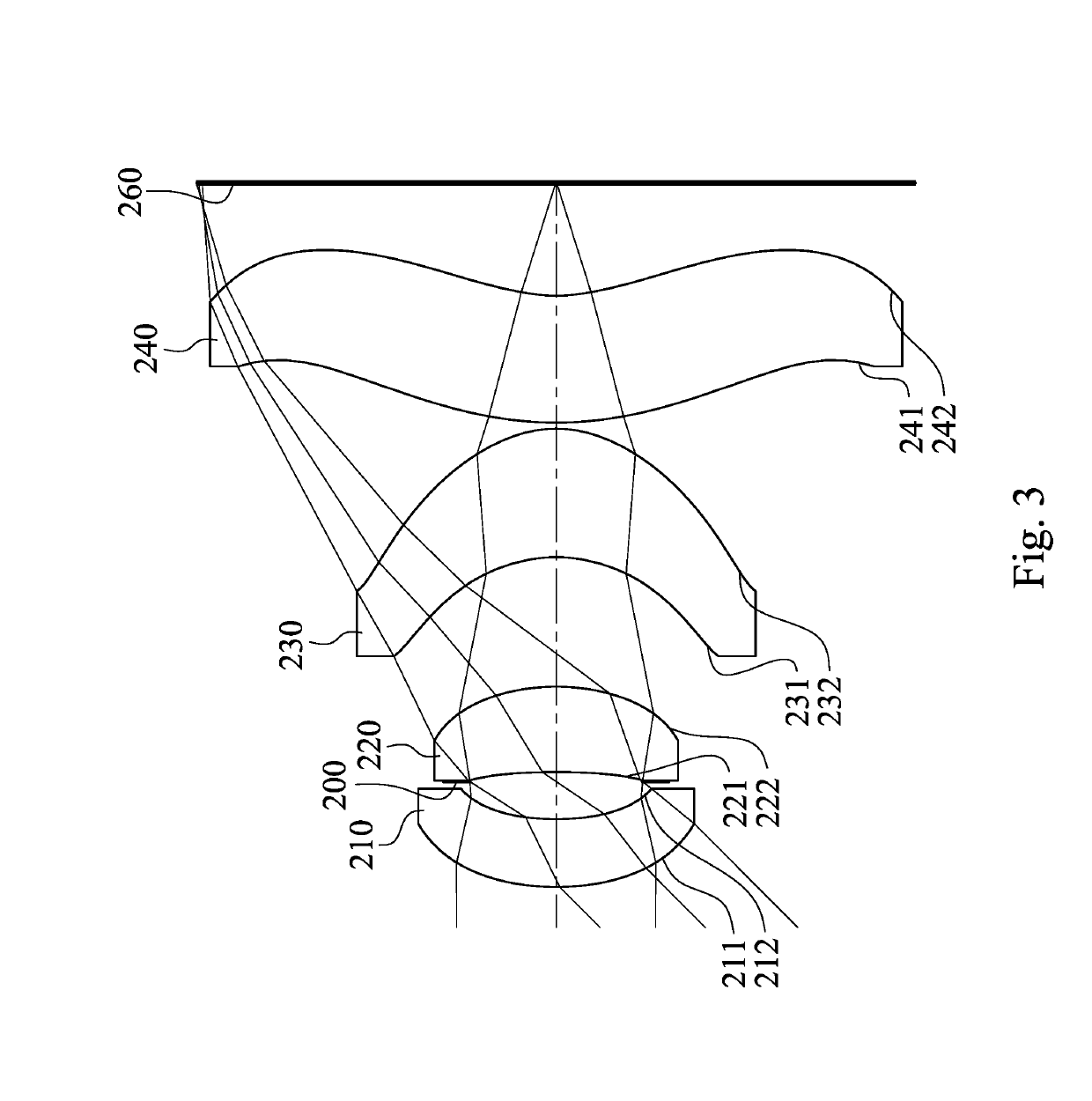
[0117]FIG. 3 is a schematic view of an electronic device according to the 2nd embodiment of the present disclosure. FIG. 4 shows spherical aberration curves, astigmatic field curves and a distortion curve of the electronic device according to the 2nd embodiment. In FIG. 3, the electronic device includes an optical lens assembly (its reference numeral is omitted), wherein the optical lens assembly includes, in order from an outside to an inside, a first lens element 210, an aperture stop 200, a second lens element 220, a third lens element 230, a fourth lens element 240 and an inside conjugation surface 260. The optical lens assembly includes four lens elements (210, 220, 230 and 240) without additional one or more lens elements inserted between the first lens element 210 and the fourth lens element 240.

[0118]The first lens element 210 with positive refractive power has an outside surface 211 being convex in a paraxial region thereof and an inside surface 212 being concave in a parax...

3rd embodiment

[0125]FIG. 5 is a schematic view of an electronic device according to the 3rd embodiment of the present disclosure. FIG. 6 shows spherical aberration curves, astigmatic field curves and a distortion curve of the electronic device according to the 3rd embodiment. In FIG. 5, the electronic device includes an optical lens assembly (its reference numeral is omitted), wherein the optical lens assembly includes, in order from an outside to an inside, a first lens element 310, an aperture stop 300, a second lens element 320, a third lens element 330, a fourth lens element 340 and an inside conjugation surface 360. The optical lens assembly includes four lens elements (310, 320, 330 and 340) without additional one or more lens elements inserted between the first lens element 310 and the fourth lens element 340.

[0126]The first lens element 310 with positive refractive power has an outside surface 311 being convex in a paraxial region thereof and an inside surface 312 being concave in a parax...


PUM


Abstract

An electronic device includes at least one optical lens assembly. The optical lens assembly includes four lens elements, and the four lens elements are, in order from an outside to an inside, a first lens element, a second lens element, a third lens element and a fourth lens element. The first lens element has an outside surface being convex in a paraxial region thereof. The second lens element has an inside surface being convex in a paraxial region thereof. The fourth lens element has an inside surface being concave in a paraxial region thereof, wherein at least one of an outside surface and the inside surface of the fourth lens element includes at least one critical point in an off-axis region thereof.

Description

RELATED APPLICATIONS[0001]This application claims priority to U.S. Provisional Application Ser. No. 62 / 565,173, filed Sep. 29, 2017, which is herein incorporated by reference.BACKGROUNDTechnical Field[0002]The present disclosure relates to an electronic device. More particularly, the present disclosure relates to an electronic device with at least one optical lens assembly.Description of Related Art[0003]With rapid developments of technologies, the application of photographing modules is becoming wider and wider, and the application technologies of three-dimensional space observation are also increasingly mature. Conventional three-dimensional space identification technologies are mostly limited to two-dimensional images, and can achieve three-dimensional spatial analysis functions with algorithms, however, when information of three-dimensional space of information is simplified into the two-dimensional space image, it will always result in information gaps, and limit restore result...

Claims


Application Information

Patent Timeline
Patent Type & Authority Applications(United States)
IPC IPC(8): G02B9/34G02B13/14G01B11/24H04N5/33
CPCH04N13/225H04N13/254G01B11/24G02B13/14H04N5/33G02B9/34G02B13/004G02B13/0015G03B30/00G02B7/32G02B13/0045H04N23/20H04N23/55G02B9/58
Inventor CHEN, HUNG-SHUOWU, CHIEN-HSUNKUO, TZU-CHIEH
Owner LARGAN PRECISION
Why Eureka
Try Eureka