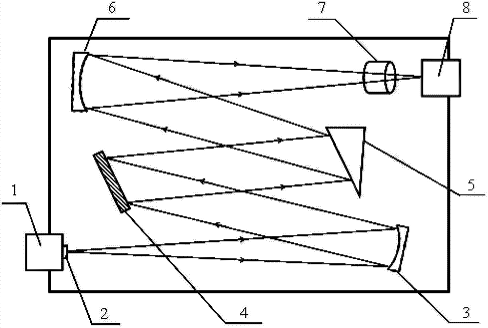
Optical path structure of small echelle grating spectrometer
An echelle grating and spectrometer technology, which is applied in the field of spectral analysis instruments, can solve problems such as low resolution, and achieve high spectral resolution, fast detection speed, and easy modularization.
- Summary
- Abstract
- Description
- Claims
- Application Information
AI Technical Summary
Problems solved by technology
Method used
Image
Examples
Embodiment 1
[0019] In the optical path structure of the present invention, both the collimating mirror 3 and the focusing mirror 6 are spherical mirrors, the radius of curvature is 200.76mm, the off-axis angles are 5.2° and 8.63° respectively, and the focal length is 100mm; the echelle grating 4 adopts a grating constant d is 1 / 54.49mm reflective engraved echelle grating, and the incident angle is 46°; for the convenience of optical path arrangement, the echelle grating is rotated 3° along the normal direction of the optical axis (that is, grating deflection angle: γ=3°); The cross-dispersion prism 5 is composed of fused silica with a half top angle of 10°, and the incident angle is 21.01°; the area array detector 8 uses an e2v back-illuminated CCD47-10AIMA chip, with a resolution of 1024×1024 pixels and a spectral response within the range of 180-300nm very high.
[0020] Through optical design software tracing, the theoretical resolution of the light path structure of the small échelle ...
Embodiment 2
[0022] In this embodiment, the radius of curvature of the collimating mirror 3 and the focusing mirror 6 in the optical path structure of the invention is changed to 200.66 mm, and the optical tracking is carried out under the condition that other structural parameters remain unchanged, and the system resolution is 0.023 nm to 200 nm.
Embodiment 3
[0024] In this embodiment, the off-axis angle of the collimating mirror 3 in the optical path structure of the invention is changed to 5.1°, and the optical tracking is performed while other structural parameters remain unchanged, and the system resolution is 0.025 nm to 200 nm.
PUM
| Property | Measurement | Unit |
|---|---|---|
| Focal length | aaaaa | aaaaa |
| Angle of incidence | aaaaa | aaaaa |
Abstract
Description
Claims
Application Information
