Method for obtaining biometric information and electronic device thereof

a biometric information and electronic device technology, applied in the direction of static indicating devices, instruments, diagnostic recording/measuring, etc., can solve the problems of slow progress of degradation of fingerprint sensor performance, sensitivity of fingerprint sensor, and performance degradation of fingerprint sensor, so as to increase the luminance of a partial region, improve the fingerprint recognition rate, and improve the effect of fingerprint recognition ra

Active Publication Date: 2019-04-18
SAMSUNG ELECTRONICS CO LTD
View PDF2 Cites 24 Cited by
  • Summary
  • Abstract
  • Description
  • Claims
  • Application Information

AI Technical Summary

Benefits of technology

[0007]To increase a fingerprint recognition rate, the electronic device can increase a luminance of a partial region of the display providing light to the fingerprint sensor compared to a luminance of the remaining region of the display, or use a light source image of a specific color. However, because the lives of light emitting elements disposed in the display are identical with each other, when the display is used continuously, the partial region of the display can be in fast progress of degradation compared to the remaining region of the display. In accordance with a degradation speed difference, a luminance difference or color deviation between the partial region and the remaining region can occur. This can be acknowledged as an afterimage to a user. Also, as a use time increases, a luminance of a light source part gradually decreases and accordingly, a sensitivity of the fingerprint sensor can deteriorate and thus the performance of the fingerprint sensor can gradually deteriorate. Therefore, higher luminance than necessary may have to be applied, in consideration of degradation. In that case, there is a danger of unnecessarily emitting too much light and accelerating the degradation. Therefore, as time goes, the luminance is increased as much as gradual degradation, whereby a specific performance can be guaranteed as a light source and even the degradation can be minimized. The control of the luminance is implemented by the control of data (i.e., a gradation value), so it can be controlled more conveniently than controlling the entire panel driving voltage.
[0008]Various embodiments of the present disclosure may provide an apparatus and method for compensating or retarding a degradation of a display providing light to a fingerprint sensor in an electronic device.

Problems solved by technology

However, because the lives of light emitting elements disposed in the display are identical with each other, when the display is used continuously, the partial region of the display can be in fast progress of degradation compared to the remaining region of the display.
Also, as a use time increases, a luminance of a light source part gradually decreases and accordingly, a sensitivity of the fingerprint sensor can deteriorate and thus the performance of the fingerprint sensor can gradually deteriorate.
In that case, there is a danger of unnecessarily emitting too much light and accelerating the degradation.

Method used


Image

  • Method for obtaining biometric information and electronic device thereof
  • Method for obtaining biometric information and electronic device thereof
  • Method for obtaining biometric information and electronic device thereof

Examples


Embodiment Construction

[0026]Various embodiments of the present disclosure are mentioned below in detail with reference to the accompanying drawings. And, in describing various embodiments of the present disclosure, related well-known functions or constructions are not described in detail for clarity and simplicity, since they would obscure the gist of the invention in unnecessary detail. And, the terms described below are defined considering functions in the present disclosure, and may be modified in accordance to user and operator's intention or practice. Therefore, the definition should be given on the basis of the content throughout the present specification.

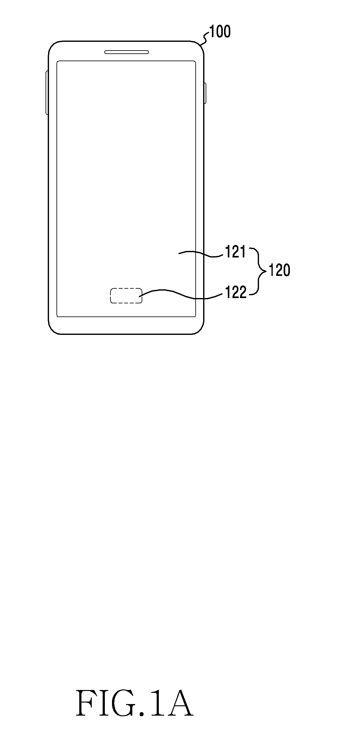
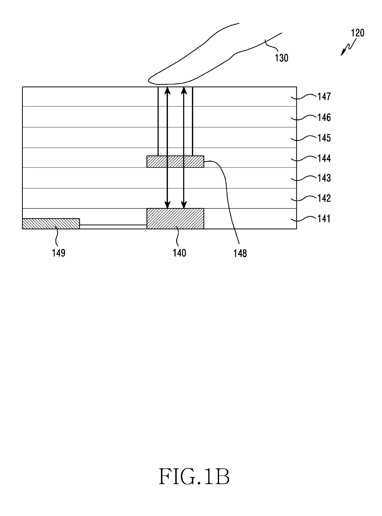
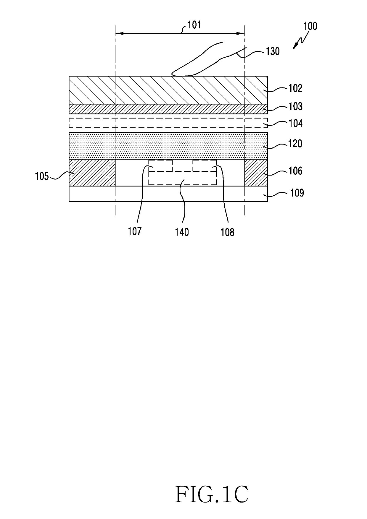
[0027]FIG. 1A to FIG. 1E illustrate schematic structures of an electronic device according to various embodiments of the present disclosure.

[0028]Referring to FIG. 1A, the electronic device 100 may include a display 120. For example, the display 120 may include a first region 121 and a second region 122.

[0029]According to an embodiment, the displa...


PUM


Abstract

An apparatus and method for obtaining biometric information in an electronic device are provided. An electronic device comprising a display comprising a plurality of pixels, a biometric sensor disposed in at least a partial region of the display; and at least one processor, wherein the at least one processor is configured to receive an input for sensing biometric information of an external object, in response to the input, select at least one pixel among a first pixel and a second pixel in accordance with history information about use of the first pixel and second pixel, wherein the first pixel and the second pixel are disposed in the at least the partial region of the display proximate to the biometric sensor, and obtain the biometric information of an external object through the biometric sensor by using light irradiated by the selected at least one pixel.

Description

CROSS-REFERENCE TO RELATED APPLICATION(S)[0001]This application is based on and claims priority under 35 U.S.C. § 119 to Korean Patent Application No. 10-2017-0133121, filed on Oct. 13, 2017, in the Korean Intellectual Property Office, the disclosure of which is incorporated by reference herein in its entirety.BACKGROUND1. Field[0002]Various embodiments of the present disclosure relate to an apparatus and method for obtaining biometric information by using a display as a light source in an electronic device.2. Description of Related Art[0003]With the growth of information and communication technology and semiconductor technology, various electronic devices are developing into multimedia devices providing various multimedia services. For example, the multimedia service can include at least one of a voice call service, a message service, a broadcasting service, a wireless Internet service, a camera service, an electronic payment service or a music play service.[0004]As the multimedia ...

Claims


Application Information

Patent Timeline
Patent Type & Authority Applications(United States)
IPC IPC(8): G06K9/00G06K9/20G06V10/141
CPCG06K9/0004G06K9/0002G06K9/2027G06K9/2036G06F3/042G06F3/0412G06F3/044G06V40/1318G06V10/17G06V10/141H04M1/72454A61B5/1171H04M2250/12G09G3/20G06V40/1306
Inventor CHO, JOUNG-MINKWON, OH HYUCKKIM, TAESUNGKIM, HYUNGDALSHIN, HYUNCHANGJUNG, SONG HEEPARK, JEONG-MINBYEON, HYUNGSUPSHIN, HEUNG-SIK
Owner SAMSUNG ELECTRONICS CO LTD
Why Eureka
Try Eureka