Check patentability & draft patents in minutes with Patsnap Eureka AI!

Stacked memory device using base die spare cell and method of repairing the same

a memory device and spare cell technology, applied in the field of repairing a stacked memory device, can solve problems such as the inability to repair a die, and achieve the effect of solving time wasted and high repair ra

Active Publication Date: 2019-06-13
IND ACADEMIC CORP FOUND YONSEI UNIV
View PDF1 Cites 3 Cited by
  • Summary
  • Abstract
  • Description
  • Claims
  • Application Information

AI Technical Summary

Benefits of technology

The patent text describes a method for improving memory repair rates by adding spare cells in the base die of a memory module and in each memory layer. These spare cells can be used for a post-bond test and repair process, which eliminates the need for a new test when the power of a memory is blocked. The method also allows for a high repair rate by permanently storing the repair result after the test. The technical effects of this method include reducing testing time and improving repair efficiency.

Problems solved by technology

In the self-repairable die, all of the faults within a die may be repaired by using an autonomously embedded spare cell, but in the repairable die using a shared spare cell, it is impossible to repair a die by using only an autonomous embedded spare cell, so that a spare cell of an adjacent die needs to be additionally used.

Method used


Image

  • Stacked memory device using base die spare cell and method of repairing the same
  • Stacked memory device using base die spare cell and method of repairing the same
  • Stacked memory device using base die spare cell and method of repairing the same

Examples


Embodiment Construction

[0027]Hereinafter, in the description of the present invention, a detailed description of known functions incorporated herein is obvious to those skilled in the art and will be omitted to avoid making the subject matter of the present invention unclear, and some exemplary embodiments of the present invention will be described in detail with reference to the illustrative drawings.

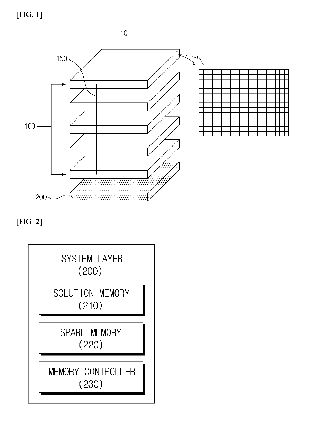
[0028]FIG. 1 is a diagram illustrating an example of a structure of a stacked memory device. The stacked memory device means a three-dimensional computer memory including one or more combined memory die layers, memory packages, or other memory elements. Referring to FIG. 1, the stacked memory device 10 may include a plurality of memory layers 100 and a system layer 200, and may be implemented on a substrate.

[0029]The stacked memory device 10 may include memory elements which are vertically stacked or horizontally stacked (for example, side-by side), or are combined with each other. The plurality of memory la...


PUM


Abstract

Disclosed are a stacked memory device and a method of repairing the same, in which spare cells for a post-bond test and repair process are disposed in a base die and the spare cells are used in each memory layer as many as the number desired, a repair result after the test is permanently stored, and the spare cell of the base die and the memory layer are simultaneously approached and meaningful data is selected, so that it is not necessary to newly perform a test even though power of a memory is blocked, it is possible to solve time wasted during an approach to a memory layer after a spare memory performs determination, and it is possible to secure a high repair rate.

Description

CROSS-REFERENCE TO RELATED APPLICATIONS[0001]This application claims priority to and the benefit of Korean Patent Application No. 10-2017-0170045 filed in the Korean Intellectual Property Office on Dec. 12, 2017, the entire contents of which are incorporated herein by reference.TECHNICAL FIELD[0002]The technical field to which the present exemplary embodiment belongs relates to a method of repairing a stacked memory device. This research was conducted as a research result of the future semiconductor device fundamental technology development program supported by the Ministry of Trade, Industry & Energy (MOTIE, 10052875) and Korea Semiconductor Research Consortium (KSRC) (No. 2017-11-1235).BACKGROUND ART[0003]Contents described herein simply provide background information about the present exemplary embodiment, but do not configure the related art.[0004]As a three-dimensional memory in which a layer of a memory is stacked is developed from a two-dimensional memory, a high repair rate ...

Claims


Application Information

Patent Timeline
Patent Type & Authority Applications(United States)
IPC IPC(8): G11C29/00
CPCG11C29/72G11C29/846G11C29/76G11C29/814G11C2029/5602G11C29/808G11C29/1201G11C15/04G11C5/06
Inventor KANG, SUNGHOHAN, DONG HYUN
Owner IND ACADEMIC CORP FOUND YONSEI UNIV
Features
  • R&D
  • Intellectual Property
  • Life Sciences
  • Materials
  • Tech Scout
  • Unparalleled Data Quality
  • Higher Quality Content
  • 60% Fewer Hallucinations
Learn More