Image Evaluation Method and Image Evaluation Device

a technology of image evaluation and evaluation method, applied in the field of image evaluation method and image evaluation device, can solve the problems of time and effort, difficult to acquire an image,

Active Publication Date: 2019-07-25
HITACHI HIGH-TECH CORP
View PDF0 Cites 18 Cited by
  • Summary
  • Abstract
  • Description
  • Claims
  • Application Information

AI Technical Summary

Benefits of technology

[0009]According to the above configuration, it is possible to detect a systematic defect without using a defect image and generating misinformation frequently.

Problems solved by technology

It takes time and effort to find, photograph, and acquire a pattern near the identification boundary and it is thought that it is not easy to acquire an image including the identification boundary surface, particularly, a defect pattern image, even if past data is used.

Method used


Image

  • Image Evaluation Method and Image Evaluation Device
  • Image Evaluation Method and Image Evaluation Device
  • Image Evaluation Method and Image Evaluation Device

Examples


Embodiment Construction

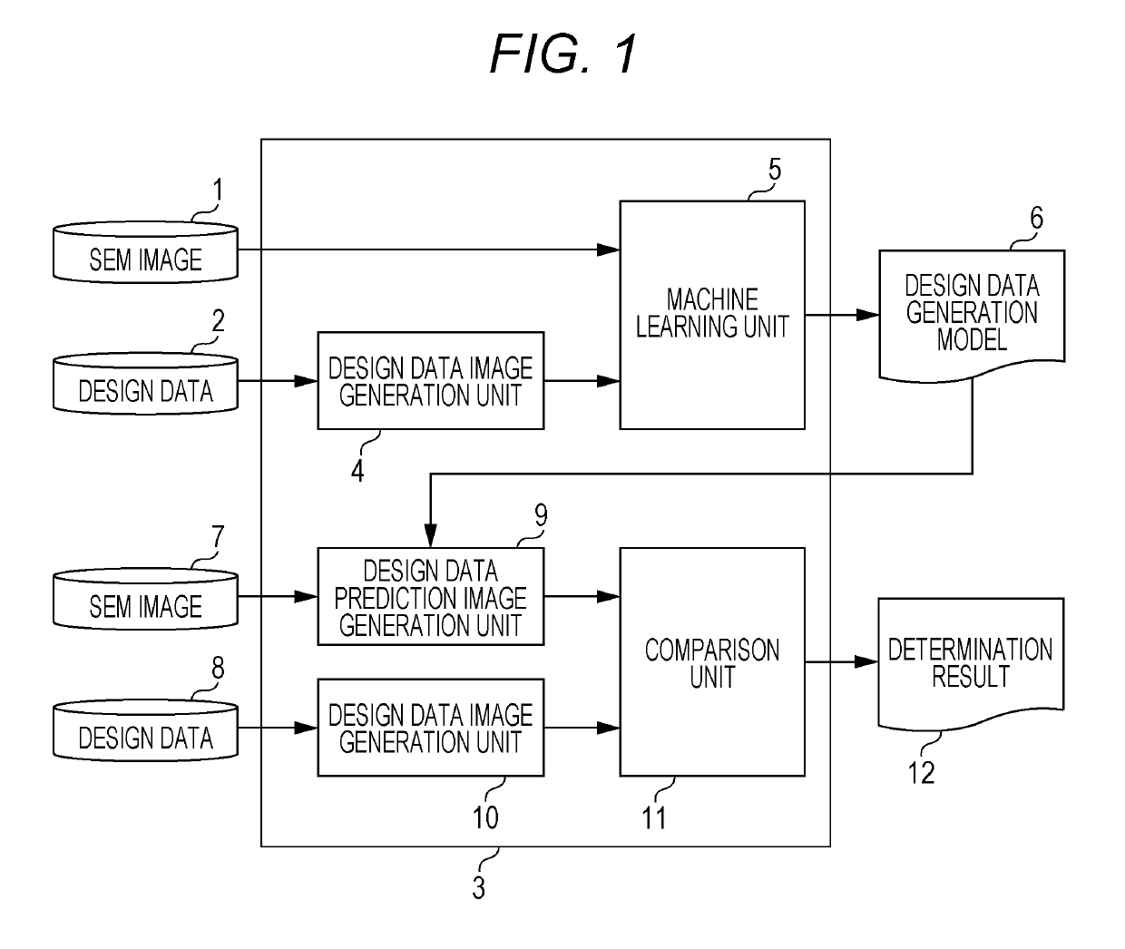
[0037]An image evaluation device exemplified in an embodiment described below relates to an image evaluation method and an image evaluation device for detecting a systematic defect without generating misinformation frequently using an inspection target image and design data.

[0038]As a concrete example, an example of removing shape deviation by returning an inspection target image to a design data image using machine learning and detecting a defect by shape comparison with the design data image is shown.

[0039]Hereinafter, a device and a measurement and inspection system having a function of detecting the systematic defect without generating the misinformation frequently using the inspection target image and the design data will be described using the drawings.

[0040]More specifically, a device and a system including a critical dimension-scanning electron microscope (CD-SEM) that is one type of measurement device will be described.

[0041]In the following description, a charged particle ...


PUM


Abstract

The image evaluation device includes a design data image generation unit that images design data; a machine learning unit that creates a model for generating a design data image from an inspection target image, using the design data image as a teacher and using the inspection target image corresponding to the design data image; a design data prediction image generation unit that predicts the design data image from the inspection target image, using the model created by the machine learning unit; a design data image generation unit that images the design data corresponding to the inspection target image; and a comparison unit that compares a design data prediction image generated by the design data prediction image generation unit and the design data image. As a result, it is possible to detect a systematic defect without using a defect image and generating misinformation frequently.

Description

BACKGROUND OF THE INVENTION1. Field of the Invention[0001]The present invention relates to an image evaluation method and an image evaluation device for inspecting a semiconductor pattern.2. Description of the Related Art[0002]According to miniaturization of a semiconductor circuit pattern, a resolution of an exposure apparatus reaches a limit and it becomes difficult to form a circuit pattern as designed on a wafer. In a circuit pattern formed on a semiconductor wafer, a defect such as a line width deviating from a design value, contraction occurring in a tip of the pattern, and a shape change of a corner or a base of the pattern is likely to occur. The defect is called a systematic defect and occurs commonly in all dies, so that it is difficult to detect the defect in a method of performing comparison between adjacent dies (die-to-die comparison).[0003]On the other hand, JP 2011-17705 A discloses a method of comparing an inspection target pattern with design data instead of compar...

Claims


Application Information

Patent Timeline
Patent Type & Authority Applications(United States)
IPC IPC(8): G06T7/00G06N20/00G06K9/20G06K9/03
CPCG06T7/0006G06N20/00G06K9/2054G06K9/036G06T7/001G06T2207/30148G06T2207/10061G06T2207/20084G06T2207/20081G06N3/08G06N3/045
Inventor SHINODA, SHINICHIISHIKAWA, MASAYOSHITOYODA, YASUTAKAABE, YUICHISHINDO, HIROYUKI
Owner HITACHI HIGH-TECH CORP
Why Eureka
Try Eureka