Supercharge Your Innovation With Domain-Expert AI Agents!

Display panel and display device

a display panel and display device technology, applied in the field of displays, can solve problems such as defective and broken conductors, and achieve the effect of reducing the width of the conductor, avoiding the breakage and defective of the conductor

Active Publication Date: 2019-08-01
TCL CHINA STAR OPTOELECTRONICS TECH CO LTD
View PDF1 Cites 0 Cited by
  • Summary
  • Abstract
  • Description
  • Claims
  • Application Information

AI Technical Summary

Benefits of technology

This patent is about a display panel and device that prevents conductors from breaking or becoming defective, especially when the panel has limited space or the number of conductors is regular. The invention achieves this by connecting two conductors on different substrates, which prevents the conductor from the thin film transistor array substrate from being transferred to the color filter substrate and potentially breaking or becoming defective. This improves the reliability and durability of the display panel.

Problems solved by technology

However, decreasing the width of the conductor could make the conductor broken and defective.

Method used


Image

  • Display panel and display device
  • Display panel and display device

Examples


Embodiment Construction

[0031]Regarding the words used in this specification, “an embodiment” means serving as an example, instance, or illustration. In addition, in this specification and the appended claims used in the articles “a / an” in general can be interpreted to mean “one or more” unless specified otherwise or clear from context to determine a singular form.

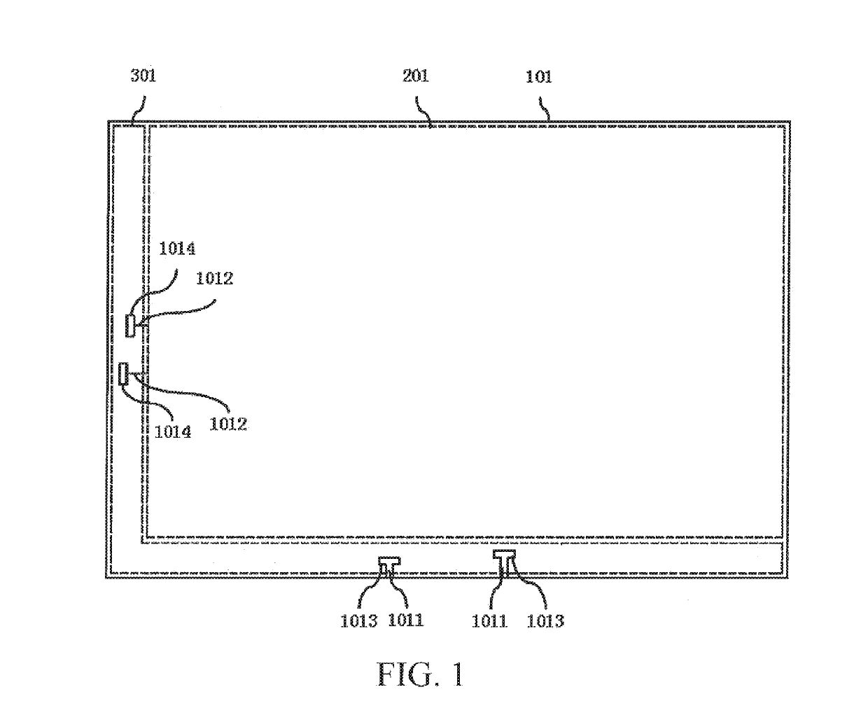
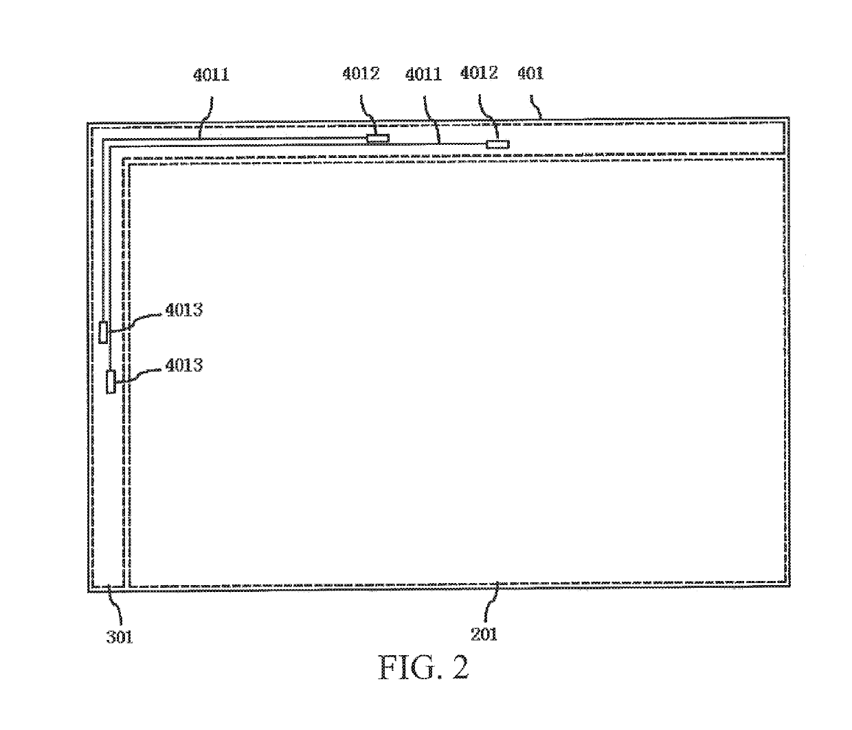
[0032]Refer to FIGS. 1 and 2, which are a schematic view of a thin film transistor array substrate 101 of a display panel of the present disclosure, and a schematic view of a color filter substrate 401 of a display panel of the present disclosure.

[0033]A display device of the present disclosure comprises a backlight module and a display panel, wherein the display panel is a TFT-LCD (Thin Film Transistor Liquid Crystal Display).

[0034]A first embodiment of the display panel of the present disclosure is disposed with a display region 201 and a peripheral region 301, wherein the peripheral region 301 is formed on at least one side of the display regi...


PUM

PropertyMeasurementUnit
areaaaaaaaaaaa
conductoraaaaaaaaaa
elastic conductiveaaaaaaaaaa

Abstract

A display panel and a display device are provided. The display panel has a thin film transistor array substrate, a color filter substrate, and a liquid crystal layer. An area of the thin film transistor array substrate corresponding to the peripheral region of the display panel is disposed with a first conductor and a conductive member, and an area of the color filter substrate corresponding to the peripheral region is disposed with a second conductor for connecting to the first conductor and the conductive member. The present disclosure can avoid the conductor being broken and defective from decreasing the width of the conductor.

Description

FIELD OF THE INVENTION[0001]The present disclosure relates to a technical field of displays, and in particular to a display panel and a display device.BACKGROUND OF THE INVENTION[0002]Traditional display panels typically include a combination of a display device and conductors, the display device is disposed in a display region of the display panel, and the conductors are disposed in a peripheral region of the display panel.[0003]A combination of the conductors has a predetermined number of conductors, and the conductors are electrically connected to the display device. The conductors are configured to transmit electrical signals to the display device.[0004]In the case which the size of the display region is increased, the size of the peripheral region could be decreased, and the width of the conductor needs to be decreased to dispose a predetermined number of the conductors. However, decreasing the width of the conductor could make the conductor broken and defective.[0005]As a resu...

Claims


Application Information

Patent Timeline
Patent Type & Authority Applications(United States)
IPC IPC(8): G02F1/1335H01L27/12G02F1/1343G02F1/133
CPCG02F1/133514H01L27/1214G02F1/1343G02F1/13306G02F1/1345G02F1/13452H01L27/124G02F1/1339
Inventor ZHAO, LIXU, XIANGYANG
Owner TCL CHINA STAR OPTOELECTRONICS TECH CO LTD
Features
  • R&D
  • Intellectual Property
  • Life Sciences
  • Materials
  • Tech Scout
  • Unparalleled Data Quality
  • Higher Quality Content
  • 60% Fewer Hallucinations
Learn More