High pressure and high temperature anneal chamber

a technology of anneal chamber and high temperature, applied in the direction of furnaces, lighting and heating apparatus, furnace types, etc., can solve the problems of reducing the spatial dimension of structural features and the difficulty of filling the gap with material

Active Publication Date: 2019-08-01
APPLIED MATERIALS INC
View PDF0 Cites 20 Cited by
  • Summary
  • Abstract
  • Description
  • Claims
  • Application Information

AI Technical Summary

Benefits of technology

The patent text describes an apparatus and method for annealing semiconductor substrates by heating them in a processing chamber. The method includes using a gas panel to provide a processing fluid, a temperature-controlled fluid circuit to maintain the processing fluid at a temperature above its condensation point, and a condenser to condense the processing fluid. The technical effects of this invention include achieving improved annealing results and reducing damage to the substrates during processing.

Problems solved by technology

Increasing device densities have resulted in structural features having decreased spatial dimensions.
For example, the aspect ratio (ratio of depth to width) of gaps and trenches forming the structural features of modern semiconductor devices have narrowed to a point where filling the gap with material has become extremely challenging.

Method used


Image

  • High pressure and high temperature anneal chamber
  • High pressure and high temperature anneal chamber
  • High pressure and high temperature anneal chamber

Examples


Embodiment Construction

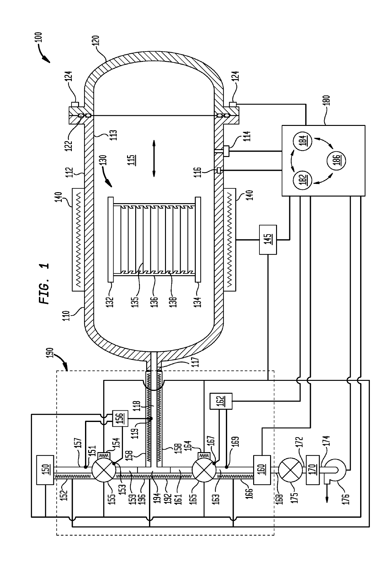
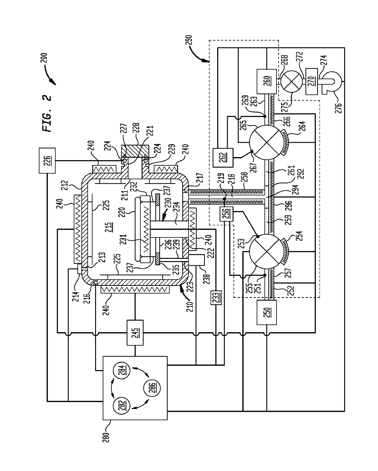
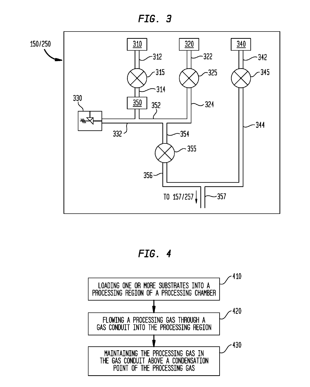
[0016]Embodiments of the disclosure relate to an apparatus and method for annealing one or more semiconductor substrates. The substrates may be annealed as a single substrate or in batches inside a single chamber. The substrates are exposed to a processing fluid under high pressure at a high temperature during annealing. The processing fluid is flowed from a gas panel through a temperature-controlled fluid circuit into a chamber when the one or more substrates are processed. The processing fluid is maintained at a temperature above the condensation point of the processing fluid by one or more heaters coupled to the fluid circuit. The fluid circuit is coupled to a condenser, where the processing fluid is condensed into liquid phase after annealing is complete. The heaters on the fluid circuit are controlled using information from temperature measurements obtained through temperature sensors interfaced with different portions of the fluid circuit. A batch processing chamber 100 shown ...


PUM


Abstract

Embodiments of the disclosure relate to an apparatus and method for annealing one or more semiconductor substrates. In one embodiment, a processing chamber is disclosed. The processing chamber includes a chamber body enclosing an internal volume, a substrate support disposed in the internal volume and configured to support a substrate during processing, a gas panel configured to provide a processing fluid into the internal volume, and a temperature-controlled fluid circuit configured to maintain the processing fluid at a temperature above a condensation point of the processing fluid. The temperature-controlled fluid circuit includes a gas conduit fluidly coupled to a port on the chamber body at a first end and to the gas panel at a second end.

Description

CROSS-REFERENCE TO RELATED APPLICATIONS[0001]This application is a divisional of U.S. patent application Ser. No. 15 / 681,317, filed Aug. 18, 2017, which is herein incorporated by reference.BACKGROUNDField[0002]Embodiments of the disclosure generally relate to fabrication of integrated circuits and particularly to an apparatus and method for annealing one or more semiconductor substrates.Description of the Related Art[0003]Formation of a semiconductor device, such as memory devices, logic devices, microprocessors etc. involves deposition of one or more films over a semiconductor substrate. The films are used to create the circuitry required to manufacture the semiconductor device. Annealing is a heat treatment process used to achieve various effects on the deposited films to improve their electrical properties. For example, annealing can be used to activate dopants, densify the deposited films, or change states of grown films.[0004]Semiconductor device geometries have dramatically de...

Claims


Application Information

Patent Timeline
Patent Type & Authority Applications(United States)
IPC IPC(8): H01L21/67H01L21/677F27B9/36H01L21/324
CPCH01L21/67109H01L21/67754F27B9/36H01L21/67248H01L21/67017H01L21/324H01L21/6719H01L21/67748
Inventor DELMAS, JEANVERHAVERBEKE, STEVENLESCHKIES, KURTIS
Owner APPLIED MATERIALS INC
Why Eureka
Try Eureka