System and method for detecting defects in an electronic device

Inactive Publication Date: 2019-08-22
ASM TECH SINGAPORE PTE LTD
View PDF23 Cites 2 Cited by
  • Summary
  • Abstract
  • Description
  • Claims
  • Application Information

AI Technical Summary

Benefits of technology

[0007]It is thus an object of the invention to seek to provide a system and method for detec

Problems solved by technology

However, if there are defects that are not found on the surfaces of the electronic device but inside the device body, optical apparatus using visible light for inspecting would not be able to locate such defects inside the device body.
Moreover, even though blemishes may appear at side surfaces of the electronic devices, it is difficult to distinguish if such blemishes are true defects or just acceptable surface scratches.
However, the aforesaid approach can only highlight part of a crack, and the extent of the crack that is highlighted depends on an angle of the cracked surface relative to the incident infrared rays.
If the infrared rays can

Method used


Image

  • System and method for detecting defects in an electronic device
  • System and method for detecting defects in an electronic device
  • System and method for detecting defects in an electronic device

Examples


Example

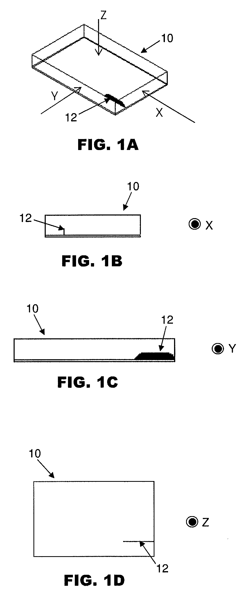
[0019]FIGS. 1A to 1D illustrate different views of an electronic device 10 illustrating how an internal defect 12 in an electronic device, such as a crack, may be detected using the system and method according to the preferred embodiment of the invention. In general, FIG. 1A shows the various views from which the electronic device 10 is inspected from the X, Y and Z directions.

[0020]FIG. 1B is a view of the electronic device 10 from the X direction or axis of FIG. 1A. From the X direction, the defect 12 is too thin to be detected, and thus may be missed. FIG. 1C is a view of the electronic device 10 from the Y direction or axis of FIG. 1A. From the Y direction, the defect 12 is more apparent, such that the electronic device 10 may be recognized as being defective. Finally, FIG. 1D is a view of the electronic device 10 from the Z direction or axis of FIG. 1A. From the Z direction, the defect 12 is again too thin to be detected, and the defect 12 may also be missed when the electronic...


PUM


Abstract

Defects in an electronic device are detected by capturing a first image from a first side of the electronic device, and capturing a second image from a second side of the electronic device which is different from the first side. The first and second images are captured when an inside of the electronic device is illuminated by light rays passed therethrough. If a defect is present in the electronic device, a profile of the defect is determined based on the first and second images and the electronic device is rejected if it is assessed from the profile of the defect that it is of a type for which the electronic device should be rejected.

Description

FIELD OF THE INVENTION[0001]The invention relates to the inspection of electronic devices, in particular to the inspection of defects in electronic devices.BACKGROUND AND PRIOR ART[0002]Defects in electronic devices, such as in wafer level electronic devices, are typically inspected by a high magnification visible light microscope adapted for viewing visible light. In a final packaging process, the electronic devices usually need to undergo visual inspection and checking so as to ensure that the devices are free from damage before packaging. However, if there are defects that are not found on the surfaces of the electronic device but inside the device body, optical apparatus using visible light for inspecting would not be able to locate such defects inside the device body. Moreover, even though blemishes may appear at side surfaces of the electronic devices, it is difficult to distinguish if such blemishes are true defects or just acceptable surface scratches.[0003]To be able to ins...

Claims


Application Information

Patent Timeline
IPC IPC(8): G01R31/265G01R31/308
CPCG01R31/2656G01R31/308
Inventor LAU, CHUNG YANCHENG, CHI WAH
Owner ASM TECH SINGAPORE PTE LTD
Why Eureka
Try Eureka